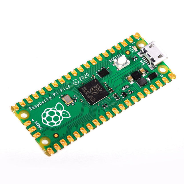
Specifications
RP2040 microcontroller chip designed by Raspberry Pi in the UK
Dual-core ARM Cortex M0+ processor, with a flexible clock running up to 133 MHz
264 kB SRAM, and 2 MB on-board Flash memory
Castellated module allows soldering directly to carrier boards
USB 1.1 host and device support
Energy-efficient sleep and dormant modes
Drag and drop programming using mass storage via USB
26x multifunction GPIO pins
2x SPI, 2x I²C, 2x UART, 3x 12-bit ADC, 16x controllable PWM channels
On-chip accurate clock and timer
Temperature sensor
On-chip accelerated floating point libraries
8x programmable IO (PIO) state machines for custom peripherals
Why a Raspberry Pi Pico?
Designing your own microcontroller instead of buying an existing one brings a number of advantages. According to Raspberry Pi itself, not one of the existing products available for this comes close to their price/performance ratio.
This Raspberry Pi Pico has also given Raspberry Pi the ability to add some innovative and powerful features of their own. These features are not available anywhere else.
A third reason is that the Raspberry Pi Pico has given Raspberry Pi the ability to create powerful software around the product. Surrounding this software stack is an extensive documentation set. The software and documentation meet the high standard of Raspberry Pi's core products (such as the Raspberry Pi 400, Pi 4 Model B and Pi 3 Model A+).
Who is this microcontroller for?
The Raspberry Pi Pico is suitable for both advanced and novice users. From controlling a display to controlling many different devices that you use every day. Automating everyday operations is made possible by this technology.
Beginner users
The Raspberry Pi Pico is programmable in the C and MicroPython languages and is customizable for a wide range of devices. In addition, the Pico is as easy to use as dragging and dropping files. This makes this microcontroller ideally suited for the novice user.
Advanced users
For advanced users, it is possible to take advantage of the Pico's extensive peripherals. The peripherals include the SPI, I²C, and eight programmable I/O (PIO)-state machines.
What makes the Raspberry Pi Pico unique?
What's unique about the Pico is that it was developed by Raspberry Pi itself. The RP2040 features a dual-core Arm Cortex-M0+ processor with 264 KB of internal RAM and support for up to 16 MB of off-chip Flash.
The Raspberry Pi Pico is unique for several reasons:
The product has the highest price/quality ratio in the microcontroller board market.
The Raspberry Pi Pico has been developed by Raspberry Pi itself.
The software stack surrounding this product is of high quality and comes paired with a comprehensive documentation set.
ESP32-C3-DevKitM-1 is an entry-level development board based on ESP32-C3-MINI-1, a module named for its small size. This board integrates complete Wi-Fi and Bluetooth LE functions. Most of the I/O pins on the ESP32-C3-MINI-1 module are broken out to the pin headers on both sides of this board for easy interfacing. Developers can either connect peripherals with jumper wires or mount ESP32-C3-DevKitM-1 on a breadboard. Specifications ESP32-C3-MINI-1 ESP32-C3-MINI-1 is a general-purpose Wi-Fi and Bluetooth LE combo module that comes with a PCB antenna. At the core of this module is ESP32-C3FN4, a chip that has an embedded flash of 4 MB. Since flash is packaged in the ESP32-C3FN4 chip, rather than integrated into the module, ESP32-C3-MINI-1 has a smaller package size. 5 V to 3.3 V LDO Power regulator that converts a 5 V supply into a 3.3 V output. 5 V Power On LED Turns on when the USB power is connected to the board. Pin Headers All available GPIO pins (except for the SPI bus for flash) are broken out to the pin headers on the board. For details, please see Header Block. Boot Button Download button. Holding down Boot and then pressing Reset initiates Firmware Download mode for downloading firmware through the serial port. Micro-USB Port USB interface. Power supply for the board as well as the communication interface between a computer and the ESP32-C3FN4 chip. Reset Button Press this button to restart the system. USB-to-UART Bridge Single USB-UART bridge chip provides transfer rates up to 3 Mbps. RGB LED Addressable RGB LED, driven by GPIO 8. Downloads ESP32-C3 Datasheet ESP32-C3-MINI-1 Datasheet ESP32-C3-DevKitM-1 Schematic ESP32-C3-DevKitM-1 PCB Layout ESP32-C3-DevKitM-1 Dimensions
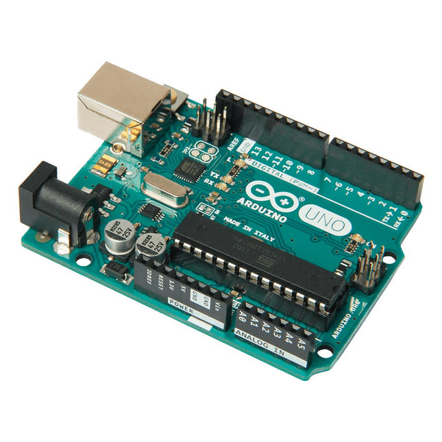
Arduino Uno is an open-source microcontroller board based on the ATmega328P. It has 14 digital input/output pins (of which 6 can be used as PWM outputs), 6 analog inputs, a 16 MHz ceramic resonator (CSTCE16M0V53-R0), a USB connection, a power jack, an ICSP header and a reset button. It contains everything needed to support the microcontroller; simply connect it to a computer with a USB cable or power it with a AC-to-DC adapter or battery to get started. You can tinker with your Uno without worring too much about doing something wrong, worst case scenario you can replace the chip for a few dollars and start over again.
'Uno' means one in Italian and was chosen to mark the release of Arduino Software (IDE) 1.0. The Uno board and version 1.0 of Arduino Software (IDE) were the reference versions of Arduino, now evolved to newer releases. The Uno board is the first in a series of USB Arduino boards, and the reference model for the Arduino platform; for an extensive list of current, past or outdated boards see the Arduino index of boards.
Specifications
Microcontroller
ATmega328P
Operating Voltage
5 V
Input Voltage (recommended)
7-12 V
Input Voltage (limit)
6-20 V
Digital I/O Pins
14 (of which 6 provide PWM output)
PWM Digital I/O Pins
6
Analog Input Pins
6
DC Current per I/O Pin
20 mA
DC Current for 3.3 V Pin
50 mA
Flash Memory
32 KB (ATmega328P) of which 0.5 KB used by bootloader
SRAM
2 KB (ATmega328P)
EEPROM
1 KB (ATmega328P)
Clock Speed
16 MHz
LED_BUILTIN
13
Dimensions
68.6 x 53.4 mm
Weight
25 g
Features
Build in USB to Serial interface
Build-in PCB antenna
Powered by Pineseed BL602 SoC using Pinenut model: 12S stamp
2 MB Flash
USB-C connection
Suitable to breadboard BIY project
On board three color LEDs output
Dimensions: 25.4 x 44.0 mm
Note: USB cable is not included.
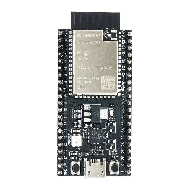
ESP32-S2-Saola-1R is a small-sized ESP32-S2 based development board. Most of the I/O pins are broken out to the pin headers on both sides for easy interfacing. Developers can either connect peripherals with jumper wires or mount ESP32-S2-Saola-1R on a breadboard.
ESP32-S2-Saola-1R is equipped with the ESP32-S2-WROVER module, a powerful, generic Wi-Fi MCU module that has a rich set of peripherals. It is an ideal choice for a wide variety of application scenarios relating to Internet of Things (IoT), wearable electronics and smart home. The board a PCB antenna and features a 4 MB external SPI flash and an additional 2 MB SPI Pseudo static RAM (PSRAM).
Features
MCU
ESP32-S2 embedded, Xtensa® single-core 32-bit LX7 microprocessor, up to 240 MHz
128 KB ROM
320 KB SRAM
16 KB SRAM in RTC
WiFi
802.11 b/g/n
Bit rate: 802.11n up to 150 Mbps
A-MPDU and A-MSDU aggregation
0.4 µs guard interval support
Center frequency range of operating channel: 2412 ~ 2484 MHz
Hardware
Interfaces: GPIO, SPI, LCD, UART, I²C, I²S, Camera interface, IR, pulse counter, LED PWM, TWAI (compatible with ISO 11898-1), USB OTG 1.1, ADC, DAC, touch sensor, temperature sensor
40 MHz crystal oscillator
4 MB SPI flash
Operating voltage/Power supply: 3.0 ~ 3.6 V
Operating temperature range: –40 ~ 85 °C
Dimensions: 18 × 31 × 3.3 mm
Applications
Generic Low-power IoT Sensor Hub
Generic Low-power IoT Data Loggers
Cameras for Video Streaming
Over-the-top (OTT) Devices
USB Devices
Speech Recognition
Image Recognition
Mesh Network
Home Automation
Smart Home Control Panel
Smart Building
Industrial Automation
Smart Agriculture
Audio Applications
Health Care Applications
Wi-Fi-enabled Toys
Wearable Electronics
Retail & Catering Applications
Smart POS Machines
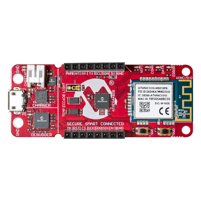
The AVR-IoT WA development board combines a powerful ATmega4808 AVR MCU, an ATECC608A CryptoAuthentication secure element IC and the fully certified ATWINC1510 Wi-Fi network controller – which provides the most simple and effective way to connect your embedded application to Amazon Web Services (AWS). The board also includes an on-board debugger, and requires no external hardware to program and debug the MCU.
Out of the box, the MCU comes preloaded with a firmware image that enables you to quickly connect and send data to the AWS platform using the on-board temperature and light sensors. Once you are ready to build your own custom design, you can easily generate code using the free software libraries in Atmel START or MPLAB Code Configurator (MCC).
The AVR-IoT WA board is supported by two award-winning Integrated Development Environments (IDEs) – Atmel Studio and Microchip MPLAB X IDE – giving you the freedom to innovate with your environment of choice.
Features
ATmega4808 microcontroller
Four user LED’s
Two mechanical buttons
mikroBUS header footprint
TEMT6000 Light sensor
MCP9808 Temperature sensor
ATECC608A CryptoAuthentication™ device
WINC1510 WiFi Module
On-board Debugger
Auto-ID for board identification in Atmel Studio and Microchip MPLAB X
One green board power and status LED
Programming and debugging
Virtual COM port (CDC)
Two DGI GPIO lines
USB and battery powered
Integrated Li-Ion/LiPo battery charger
The SparkFun RedBoard Qwiic is an Arduino-compatible board that combines features of different Arduinos with the Qwiic Connect System.
Features
ATmega328 microcontroller with Optiboot Bootloader
R3 Shield Compatible
CH340C Serial-USB Converter
3.3 V to 5 V Voltage Level Jumper
A4 / A5 Jumpers
AP2112 Voltage Regulator
ISP Header
Input voltage: 7 V - 15 V
1 Qwiic Connector
16 MHz Clock Speed
32 k Flash Memory
All SMD Construction
Improved Reset Button
LuckFox Pico Mini is a compact Linux micro development board based on the Rockchip RV1103 chip, providing a simple and efficient development platform for developers. It supports a variety of interfaces, including MIPI CSI, GPIO, UART, SPI, I²C, USB, etc., which is convenient for quick development and debugging.
Features
Single-core ARM Cortex-A7 32-bit core with integrated NEON and FPU
Built-in Rockchip self-developed 4th generation NPU, features high computing precision and supports int, int8, and int16 hybrid quantization. The computing power of int8 is 0.5 TOPS, and up to 1.0 TOPS with int4
Built-in self-developed third-generation ISP3.2, supports 4-Megapixel, with multiple image enhancement and correction algorithms such as HDR, WDR, multi-level noise reduction, etc.
Features powerful encoding performance, supports intelligent encoding mode and adaptive stream saving according to the scene, saves more than 50% bit rate of the conventional CBR mode so that the images from camera are high-definition with smaller size, double the storage space
Built-in RISC-V MCU supports low power consumption and fast start-up, supports 250 ms fast picture capture and loading Al model library at the same time to realize face recognition "in one second"
Built-in 16-bit DRAM DDR2, which is capable of sustaining demanding memory bandwidths
Integrated with built-in POR, audio codec and MAC PHY
Specifications
Processor
ARM Cortex-A7, single-core 32-bit CPU, 1.2 GHz, with NEON and FPU
NPU
Rockchip 4th-gen NPU, supports int4, int8, int16; up to 1.0 TOPS (int4)
ISP
Third-gen ISP3.2, up to 4 MP input at 30fps, HDR, WDR, noise reduction
RAM
64 MB DDR2
Storage
128 MB SPI NAND Flash
USB
USB 2.0 Host/Device via Type-C
Camera Interface
MIPI CSI 2-lane
GPIO Pins
17 GPIO pins
Power Consumption
Low power, RISC-V MCU for fast startup
Dimensions
28 x 21 mm
Downloads
Wiki
The OKdo E1 is an ultra-low-cost Development Board based on the NXP LPC55S69JBD100 dual-core Arm Cortex-M33 microcontroller. The E1 board is perfect for Industrial IoT, building control and automation, consumer electronics, general embedded and secure applications.
Features
Processor with Arm TrustZone, Floating Point Unit (FPU) and Memory Protection Unit (MPU)
CASPER Crypto co-processor to enable hardware acceleration for certain asymmetric cryptographic algorithms
PowerQuad Hardware Accelerator for fixed and floating point DSP functions
SRAM Physical Unclonable Function (PUF) for key generation, storage and reconstruction
PRINCE module for real-time encryption and decryption of flash data
AES-256 and SHA2 engines
Up to Nine Flexcomm interfaces. Each Flexcomm interface can be selected by software to be a USART, SPI, I²C, and I²S interface
USB 2.0 High-Speed Host/Device controller with on-chip PHY
USB 2.0 Full-Speed Host/Device controller with on-chip PHY
Up to 64 GPIOs
Secure digital input/output (SD/MMC and SDIO) card interface
Specifications
LPC55S69JBD100 640kbyte flash microcontroller
In-built CMSIS-DAP v1.0.7 debugger based on LPC11U35
Internal PLL support up to 100MHz operation, 16MHz can be mounted for full 150MHz operation.
SRAM 320kB
32kHz crystal for real-time clock
4 user switches
3-colour LED
User USB connector
2-off 16-way expansion connectors
UART over USB virtual COM port
The EC200U-EU C4-P01 development board features the EC200U-EU LTE Cat 1 wireless communication module, offering a maximum data rate of up to 10 Mbps for downlink and 5 Mbps for uplink. It supports multi-mode and multi-band communication, making it a cost-effective solution.
The board is designed in a compact and unified form factor, compatible with the Quectel multi-mode LTE Standard EC20-CE. It includes an onboard USB-C port, allowing for easy development with just a USB-C cable.
Additionally, the board is equipped with a 40-pin GPIO header that is compatible with most Raspberry Pi HATs.
Features
Equipped with EC200U-EU LTE Cat 1 wireless communication module, multi-mode & multi-band support
Onboard 40-Pin GPIO header, compatible with most Raspberry Pi HATs
5 LEDs for indicating module operating status
Supports TCP, UDP, PPP, NITZ, PING, FILE, MQTT, NTP, HTTP, HTTPS, SSL, FTP, FTPS, CMUX, MMS protocols, etc.
Supports GNSS positioning (GPS, GLONASS, BDS, Galileo, QZSS)
Onboard Nano SIM card slot and eSIM card slot, dual card single standby
Onboard MIPI connector for connecting MIPI screen and is fully compatible with Raspberry Pi peripherals
Onboard camera connector, supports customized SPI cameras with a maximum of 300,000 pixels
Provides tools such as QPYcom, Thonny IDE plugin, and VSCode plugin, etc. for easy learning and development
Comes with online development resources and manual (example in QuecPython)
Specifications
Applicable Regions
Europe, Middle East, Africa, Australia, New Zealand, Brazil
LTE-FDD
B1, B3, B5, B7, B8, B20, B28
LTE-TDD
B38, B40, B41
GSM / GPRS / EDGE
GSM: B2, B3, B5, B8
GNSS
GPS, GLONASS, BDS, Galileo, QZSS
Bluetooth
Bluetooth 4.2 (BR/EDR)
Wi-Fi Scan
2.4 GHz 11b (Rx)
CAT 1
LTE-FDD: DL 10 Mbps; UL 5 Mbps
LTE-TDD: DL 8.96 Mbps; UL 3.1 Mbps
GSM / GPRS / EDGE
GSM: DL 85.6 Kbps; UL 85.6 Kbps
USB-C Port
Supports AT commands testing, GNSS positioning, firmware upgrading, etc.
Communication Protocol
TCP, UDP, PPP, NITZ, PING, FILE, MQTT, NTP, HTTP, HTTPS, SSL, FTP, FTPS, CMUX, MMS
SIM Card
Nano SIM and eSIM, dual card single standby
Indicator
P01: Module Pin 1, default as EC200A-XX PWM0
P05: Module Pin 5, NET_MODE indicator
SCK1: SIM1 detection indicator, lights up when SIM1 card is inserted
SCK2: SIM2 detection indicator, lights up when SIM2 card is inserted
PWR: Power indicator
Buttons
PWK: Power ON/OFF
RST: Reset
BOOT: Forcing into firmware burning mode
USB ON/OFF: USB power consumption detection switch
Antenna Connectors
LTE main antenna + DIV / WiFi (scanning only) / Bluetooth antenna + GNSS antenna
Operating Temperature
−30~+75°C
Storage Temperature
−45~+90°C
Downloads
Wiki
Quectel Resources
The LuckFox Pico Ultra is a compact single-board computer (SBC) powered by the Rockchip RV1106G3 chipset, designed for AI processing, multimedia, and low-power embedded applications.
It comes equipped with a built-in 1 TOPS NPU, making it ideal for edge AI workloads. With 256 MB RAM, 8 GB onboard eMMC storage, integrated WiFi, and support for the LuckFox PoE module, the board delivers both performance and versatility across a wide range of use cases.
Running Linux, the LuckFox Pico Ultra supports a variety of interfaces – including MIPI CSI, RGB LCD, GPIO, UART, SPI, I²C, and USB – providing a simple and efficient development platform for applications in smart home, industrial control, and IoT.
Specifications
Chip
Rockchip RV1106G3
Processor
Cortex-A7 1.2 GHz
Neural Network Processor (NPU)
1 TOPS, supports int4, int8, int16
Image Processor (ISP)
Max input 5M @30fps
Memory
256 MB DDR3L
WiFi + Bluetooth
2.4GHz WiFi-6 Bluetooth 5.2/BLE
Camera Interface
MIPI CSI 2-lane
DPI Interface
RGB666
PoE Interface
IEEE 802.3af PoE
Speaker interface
MX1.25 mm
USB
USB 2.0 Host/Device
GPIO
30 GPIO pins
Ethernet
10/100M Ethernet controller and embedded PHY
Default Storage Medium
eMMC (8 GB)
Included
1x LuckFox Pico Ultra W
1x LuckFox PoE module
1x IPX 2.4G 2 db antenna
1x USB-A to USB-C cable
1x Screws pack
Downloads
Wiki
The Milk-V Duo 256M is an ultra-compact embedded development platform based on the SG2002 chip. It can run Linux and RTOS, providing a reliable, low-cost, and high-performance platform for professionals, industrial ODMs, AIoT enthusiasts, DIY hobbyists, and creators.
This board is an upgraded version of Duo with a memory boost to 256M, catering to applications demanding larger memory capacities. The SG2002 elevates computational power to 1.0 TOPS @ INT8. It enables seamless switching between RISC-V/ARM architectures and supports simultaneous operation of dual systems. Additionally, it includes an array of rich GPIO interfaces such as SPI, UART, suitable for a wide range of hardware development in edge intelligent monitoring, including IP cameras, smart peephole locks, visual doorbells, and more.
SG2002 is a high-performance, low-power chip designed for various product fields such as edge intelligent surveillance IP cameras, smart door locks, visual doorbells, and home intelligence. It integrates H.264 video compression and decoding, H.265 video compression encoding, and ISP capabilities. It supports multiple image enhancement and correction algorithms such as HDR wide dynamic range, 3D noise reduction, defogging, and lens distortion correction, providing customers with professional-grade video image quality.
The chip also incorporates a self-developed TPU, delivering 1.0 TOPS of computing power under 8-bit integer operations. The specially designed TPU scheduling engine efficiently provides high-bandwidth data flow for all tensor processing unit cores. Additionally, it offers users a powerful deep learning model compiler and software SDK development kit. Leading deep learning frameworks like Caffe and Tensorflow can be easily ported to its platform. Furthermore, it includes security boot, secure updates, and encryption, providing a series of security solutions from development, mass production, to product applications.
The chip integrates an 8-bit MCU subsystem, replacing the typical external MCU to achieve cost-saving and power efficiency goals.
Specifications
SoC
SG2002
RISC-V CPU
C906 @ 1 Ghz + C906 @ 700 MHz
Arm CPU
1x Cortex-A53 @ 1 GHz
MCU
8051 @ 6 KB SRAM
Memory
256 MB SIP DRAM
TPU
1.0 TOPS @ INT8
Storage
1x microSD connector or 1x SD NAND on board
USB
1x USB-C for power and data, USB Pads available
CSI
1x 16P FPC connector (MIPI CSI 2-lane)
Sensor Support
5 M @ 30 fps
Ethernet
100 Mbps Ethernet with PHY
Audio
Via GPIO Pads
GPIO
Up to 26x GPIO Pads
Power
5 V/1 A
OS Support
Linux, RTOS
Dimensions
21 x 51 mm
Downloads
Documentation
GitHub
The FRDM-MCXN947 is a compact and versatile development board designed for rapid prototyping with MCX N94 and N54 microcontrollers. It features industry-standard headers for easy access to the MCU's I/Os, integrated open-standard serial interfaces, external flash memory, and an onboard MCU-Link debugger.
Specifications
Microcontroller
MCX-N947 Dual Arm Cortex-M33 cores @ 150 MHz each with optimized performance efficiency, up to 2 MB dual-bank flash with optional full ECC RAM, External flash
Accelerators: Neural Processing Unit, PowerQuad, Smart DMA, etc.
Memory Expansion
*DNP Micro SD card socket
Connectivity
Ethernet Phy and connector
HS USB-C connectors
SPI/I²C/UART connector (PMOD/mikroBUS, DNP)
WiFi connector (PMOD/mikroBUS, DNP)
CAN-FD transceiver
Debug
On-board MCU-Link debugger with CMSIS-DAP
JTAG/SWD connector
Sensor
P3T1755 I³C/I²C Temp Sensor, Touch Pad
Expansion Options
Arduino Header (with FRDM expansion rows)
FRDM Header
FlexIO/LCD Header
SmartDMA/Camera Header
Pmod *DNP
mikroBUS
User Interface
RGB user LED, plus Reset, ISP, Wakeup buttons
Included
1x FRDM-MCXN947 Development Board
1x USB-C Cable
1x Quick Start Guide
Downloads
Datasheet
Block diagram
The CubeCell series is designed primarily for LoRa/LoRaWAN node applications.
Built on the ASR605x platform (ASR6501, ASR6502), these chips integrate the PSoC 4000 series MCU (ARM Cortex-M0+ Core) with the SX1262 module. The CubeCell series offers seamless Arduino compatibility, stable LoRaWAN protocol operation, and straightforward connectivity with lithium batteries and solar panels.
The HTCC-AB02S is a developer-friendly board with an integrated AIR530Z GPS module, ideal for quickly testing and validating communication solutions.
Features
Arduino compatible
Based on ASR605x (ASR6501, ASR6502), those chips are already integrated the PSoC 4000 series MCU (ARM Cortex M0+ Core) and SX1262
LoRaWAN 1.0.2 support
Ultra low power design, 21 uA in deep sleep
Onboard SH1.25-2 battery interface, integrated lithium battery management system (charge and discharge management, overcharge protection, battery power detection, USB/battery power automatic switching)
Good impendence matching and long communication distance
Onboard solar energy management system, can directly connect with a 5.5~7 V solar panel
Micro USB interface with complete ESD protection, short circuit protection, RF shielding, and other protection measures
Integrated CP2102 USB to serial port chip, convenient for program downloading, debugging information printing
Onboard 0.96-inch 128x64 dot matrix OLED display, which can be used to display debugging information, battery power, and other information
Using Air530 GPS module with GPS/Beidou Dual-mode position system support
Specifications
Main Chip
ASR6502 (48 MHz ARM Cortex-M0+ MCU)
LoRa Chipset
SX1262
Frequency
863~870 MHz
Max. TX Power
22 ±1 dBm
Max. Receiving Sensitivity
−135 dBm
Hardware Resource
2x UART1x SPI2x I²C1x SWD3x 12-bit ADC input8-channel DMA engine16x GPIO
Memory
128 Kb FLASH16 Kb SRAM
Power consumption
Deep sleep 21 uA
Interfaces
1x Micro USB1x LoRa Antenna (IPEX)2x (15x 2.54 Pin header) + 3x (2x 2.54 Pin header)
Battery
3.7 V lithium battery (power supply and charging)
Solar Energy
VS pin can be connected to 5.5~7 V solar panel
USB to Serial Chip
CP2102
Display
0.96" OLED (128 x 64)
Operating temperature
−20~70°C
Dimensions
55.9 x 27.9 x 9.5 mm
Included
1x CubeCell HTCC-AB02S Development Board
1x Antenna
1x 2x SH1.25 battery connector
Downloads
Datasheet
Schematic
GPS module (Manual)
Quick start
GitHub
The SparkFun RP2040 mikroBUS Development Board is a low-cost, high performance platform with flexible digital interfaces featuring the Raspberry Pi Foundation's RP2040 microcontroller. Besides the Thing Plus or Feather PTH pin layout, the board also includes a microSD card slot, 16 MB (128 Mbit) flash memory, a JST single cell battery connector (with a charging circuit and fuel gauge sensor), an addressable WS2812 RGB LED, JTAG PTH pins, four (4-40 screw) mounting holes, our signature Qwiic connectors, and a mikroBUS socket. The mikroBUS standard was developed by MikroElektronika. Similar to Qwiic and MicroMod interfaces, the mikroBUS socket provides a standardized connection for add-on Click boards to be attached to a development board and is comprised of a pair of 8-pin female headers with a standardized pin configuration. The pins consist of three groups of communications pins (SPI, UART and I²C), six additional pins (PWM, Interrupt, Analog input, Reset and Chip select), and two power groups (3.3 V and 5 V). The RP2040 is supported with both C/C++ and MicroPython cross-platform development environments, including easy access to runtime debugging. It has UF2 boot and floating-point routines baked into the chip. While the chip has a large amount of internal RAM, the board includes an additional 16 MB of external QSPI flash memory to store program code. The RP2040 contains two ARM Cortex-M0+ processors (up to 133 MHz) and features: 264 kB of embedded SRAM in six banks 6 dedicated IO for SPI Flash (supporting XIP) 30 multifunction GPIO: Dedicated hardware for commonly used peripherals Programmable IO for extended peripheral support Four 12-bit ADC channels with internal temperature sensor (up to 0.5 MSa/s) USB 1.1 Host/Device functionality Features (SparkFun RP2040 mikroBUS Dev. Board) Raspberry Pi Foundation's RP2040 microcontroller 18 Multifunctional GPIO Pins Four available 12-bit ADC channels with internal temperature sensor (500kSa/s) Up to eight 2-channel PWM Up to two UARTs Up to two I²C buses Up to two SPI buses Thing Plus (or Feather) Pin Layout: 28 PTH Pins USB-C Connector: USB 1.1 Host/Device functionality 2-pin JST Connector for a LiPo Battery (not included): 500mA charging circuit 4-pin JST Qwiic Connector LEDs:
PWR - Red 3.3V power indicator
CHG - Yellow battery charging indicator
25 - Blue status/test LED (GPIO 25)
WS2812 - Addressable RGB LED (GPIO 08) Buttons: Boot Reset JTAG PTH Pins 16MB QSPI Flash Memory µSD Card Slot mikroBUS Socket Dimensions: 3.7' x 1.2' Four Mounting Holes: 4-40 screw compatible Downloads Schematic Eagle Files Board Dimensions Hookup Guide Qwiic Info Page GitHub Hardware Repository
The ATmega328 Uno Development Board (Arduino Uno compatible) is a microcontroller board based on the ATmega328.
It has 14 digital input/output pins (of which 6 can be used as PWM outputs), 6 analogue inputs, a 16 MHz ceramic resonator, a USB connection, a power jack, an ICSP header and a reset button.
It contains everything needed to support the microcontroller; connect it to a computer with a USB cable or power it with a AC-to-DC adapter or battery to get started.
Specifications
Microcontroller
ATmega328
Operating voltage
5 V DC
Input voltage (recommended)
7-12 V DC
Input voltage (limits)
6-20 V DC
Digital I/O pins
14 (of which 6 provide PWM output)
Analogue input pins
6
SRAM
2 kB (ATmega328)
EEPROM
1 kB (ATmega328)
Flash memory
32 kB (ATmega328) of which 0.5 kB used by bootloader
Clock speed
16 MHz
Downloads
Manual
Arduino MKR NB 1500 allows you to build your next smart project.
Ever wanted an automated house? Or a smart garden? Well, now it’s easy with the Arduino IoT Cloud compatible boards. It means: you can connect devices, visualize data, control and share your projects from anywhere in the world. Whether you’re a beginner or a pro, we have a wide range of plans to make sure you get the features you need.
Add Narrowband communication to your project with the MKR NB 1500. It's the perfect choice for devices in remote locations without an Internet connection, or in situations in which power isn't available like on-field deployments, remote metering systems, solar-powered devices, or other extreme scenarios.
The board's main processor is a low power ARM Cortex-M0 32-bit SAMD21, like in the other boards within the Arduino MKR family. The Narrowband connectivity is performed with a module from u-blox, the SARA-R410M-02B, a low power chipset operating in the de different bands of the IoT LTE cellular range. On top of those, secure communication is ensured through the Microchip ECC508 crypto chip. Besides that, the pcb includes a battery charger, and a connector for an external antenna.
This board is designed for global use, providing connectivity on LTE's Cat M1/NB1 bands 1, 2, 3, 4, 5, 8, 12, 13, 18, 19, 20, 25, 26, 28. Operators offering service in that part of the spectrum include: Vodafone, AT&T, T-Mobile USA, Telstra, and Verizon, among others.
Specifications
The Arduino MKR NB 1500 is based on the SAMD21 microcontroller.
Microcontroller
SAMD21 Cortex-M0+ 32-bit low power ARM MCU (datasheet)
Radio module
u-blox SARA-R410M-02B (datasheet summary)
Secure element
ATECC508 (datasheet)
Board power supply (USB/VIN)
5 V
Supported battery
Li-Po Single Cell, 3.7 V, 1500 mAh Minimum
Circuit operating voltage
3.3 V
Digital I/O pins
8
PWM pins
13 (0 .. 8, 10, 12, 18 / A3, 19 / A4)
UART
1
SPI
1
I²C
1
Analog input pins
7 (ADC 8/10/12 bit)
Analog output pins
1 (DAC 10 bit)
External interrupts
8 (0, 1, 4, 5, 6, 7, 8, 16 / A1, 17 / A2)
DC current per I/O pin
7 mA
Flash memory
256 KB (internal)
SRAM
32 KB
EEPROM
No
Clock speed
32.768 kHz (RTC), 48 MHz
LED_BUILTIN
6
USB
Full-speed USB device and embedded host
Antenna gain
2 dB
Carrier frequency
LTE bands 1, 2, 3, 4, 5, 8, 12, 13, 18, 19, 20, 25, 26, 28
Power class (radio)
LTE Cat M1 / NB1: Class 3 (23 dBm)
Data rate (LTE M1 halp-duplex)
UL 375 kbps / DL 300 kbps
Data rate (LTE NB1 full-duplex)
UL 62.5 kbps / DL 27.2 kbps
Working region
Multiregion
Device location
GNSS via modem
Power consumption (LTE M1)
min 100 mA / max 190 mA
Power consumption (LTE NB1)
min 60 mA / max 140 mA
SIM card
MicroSIM (not included with the board)
Dimensions
67.6 x 25 mm
Weight
32 g
Downloads
Eagle Files
Schematics
Pinout
The Arduino MKR Zero is a development board for music makers! With an SD card holder and dedicated SPI interfaces (SPI1), you are able to play music files without extra hardware.
The MKR Zero brings you the power of a Zero in the smaller format established by the MKR form factor. The MKR Zero board acts as a great educational tool for learning about 32-bit application development. It has an on-board SD connector with dedicated SPI interfaces (SPI1) that allows you to play with MUSIC files with no extra hardware! The board is powered by Atmel’s SAMD21 MCU, which features a 32-bit ARM Cortex M0+ core.
The board contains everything needed to support the microcontroller; simply connect it to a computer with a micro-USB cable or power it by a LiPo battery. The battery voltage can also be monitored since a connection between the battery and the analog converter of the board exists.
Specifications
Microcontroller
SAMD21 ARM Cortex-M0+ 32-bit low power
Board power supply (USB/VIN)
5 V
Supported battery
Li-Po single cell, 3.7 V, 700 mAh minimum
DC current for 3.3 V pin
600 mA
DC current for 5 V pin
600 mA
Circuit operating voltage
3.3 V
Digital I/O pins
22
PWM pins
12 (0, 1, 2, 3, 4, 5, 6, 7, 8, 10, A3 - or 18 -, A4 -or 19)
UART
1
SPI
1
I²C
1
Analog input pins
7 (ADC 8/10/12 bit)
Analog output pins
1 (DAC 10 bit)
External interrupts
10 (0, 1, 4, 5, 6, 7, 8, A1 -or 16-, A2 - or 17)
DC current per I/O pin
7 mA
Flash memory
256 KB
Flash memory for bootloader
8 KB
SRAM
32 KB
EEPROM
No
Clock speed
32.768 kHz (RTC), 48 MHz
LED_BUILTIN
32
Downloads
Datasheet
Eagle Files
Schematics
Fritzing
Pinout
The Arduino Pro Portenta Cat. M1/NB IoT GNSS Shield allows you to enhance the connectivity features of your Portenta H7 applications. The shield leverages a Cinterion TX62 wireless module by Thales, designed for highly efficient, low-power IoT applications to deliver optimized bandwidth and performance.
The Portenta Cat. M1/NB IoT GNSS Shield combines with the strong edge computing power of the Portenta H7 to enable the development of asset tracking and remote monitoring applications in industrial settings, as well as in agriculture, public utilities and smart cities. The shield offers cellular connectivity to both Cat. M1 and NB-IoT networks with the option to use eSIM technology. Easily track your valuables – across the city or worldwide – with your choice of GPS, GLONASS, Galileo or BeiDou.
Features
Change connectivity capabilities without changing the board
Add NB-IoT, CAT. M1 and positioning to any Portenta product
Possibility to create a small multiprotocol router (WiFi - BT + NB-IoT/CAT. M1)
Greatly reduce communication bandwidth requirements in IoT applications
Low-power module
Compatible also with MKR boards
Remote Monitoring
Industrial and agricultural companies can leverage the Portenta Cat. M1/NB IoT GNSS Shield to remotely monitor gas detectors, optical sensors, machinery alarm systems, biological bug traps and more.
Technology providers providing smart city solutions can compound the power and reliability of the Portenta H7 with the Portenta Cat. M1/NB IoT GNSS Shield, to connect data and automate actions for a truly optimized use of resources and enhanced user experience.
Asset Monitoring
Add monitoring capabilities to any asset by combining the performance and edge computing features of the Portenta family boards. The Portenta Cat. M1/NB IoT GNSS Shield is ideal to monitor valuable goods and also for monitoring industrial machinery and equipment.
Specifications
Connectivity
Cinterion TX62 wireless module; NB-IoT - LTE CAT.M1; 3GPP Rel.14 Compliant Protocol LTE Cat. M1/NB1/NB2; UMTS BANDS: 1 / 2 / 3 / 4 / 5 / 8 / 12(17) / 13 / 18 / 19 / 20 / 25 / 26 / 27 / 28 / 66 / 71 / 85; LTE Cat.M1 DL: max. 300 kbps, UL: max. 1.1 Mbps; LTE Cat.NB1 DL: max. 27 kbps, UL: max. 63 kbps; LTE Cat.NB2 DL: max. 124 kbps, UL: max. 158 kbps
Short messaging service (SMS)
Point-to-point mobile terminated (MT) and mobile originated (MO) Text Mode; Protocol Data Unit (PDU) Mode
Localization support
GNSS capability (GPS/BeiDou/Galileo/GLONASS)
Other
Embedded IPv4 and IPv6 TCP/IP stack access; Internet Services: TCP server/client, UDP client, DNS, Ping, HTTP client, FTP client, MQTT client Secure Connection with TLS/DTLS Secure boot
Dimensions
66 x 25.4 mm
Operating temperature
-40° C to +85° C (-104° F to 185°F)
Downloads
Datasheet
Schematics