The SparkFun RedBoard Qwiic is an Arduino-compatible board that combines features of different Arduinos with the Qwiic Connect System.
Features
ATmega328 microcontroller with Optiboot Bootloader
R3 Shield Compatible
CH340C Serial-USB Converter
3.3 V to 5 V Voltage Level Jumper
A4 / A5 Jumpers
AP2112 Voltage Regulator
ISP Header
Input voltage: 7 V - 15 V
1 Qwiic Connector
16 MHz Clock Speed
32 k Flash Memory
All SMD Construction
Improved Reset Button
Plug a reader into the headers, use a Qwiic cable, scan your 125kHz ID tag, and the unique 32-bit ID will be shown on the screen. The unit comes with a read LED and buzzer, but don't worry, there is a jumper you can cut to disable the buzzer if you want. Utilizing SparkFun's handy Qwiic system, no soldering is required to connect it to the rest of your system. However, we still have broken out 0.1"-spaced pins if you prefer to use a breadboard.
Utilizing the onboard ATtiny84A, the Qwiic RFID takes the six byte ID tag of your 125kHz RFID card, attaches a timestamp to it, and puts it onto a stack that holds up to 20 unique RFID scans at a time. This information is easy to get at with some simple I²C commands.
The Challenger RP2040 NFC is a small embedded computer, equipped with an advanced on-board NFC controller (NXP PN7150), in the popular Adafruit Feather form factor. It is based on an RP2040 microcontroller chip from the Raspberry Pi Foundation which is a dual-core Cortex-M0 that can run on a clock up to 133 MHz.
NFC
The PN7150 is a full featured NFC controller solution with integrated firmware and NCI interface designed for contactless communication at 13.56 MHz. It is fully compatible with NFC forum requirements and is greatly designed based on learnings from previous NXP NFC device generation. It is the ideal solution for rapidly integrating NFC technology in any application, especially small embedded systems reducing Bill of Material (BOM).
The integrated design with full NFC forum compliancy gives the user all the following features:
Embedded NFC firmware providing all NFC protocols as pre-integrated feature.
Direct connection to the main host or microcontroller, by I²C-bus physical and NCI protocol.
Ultra-low power consumption in polling loop mode.
Highly efficient integrated power management unit (PMU) allowing direct supply from a battery.
Specifications
Microcontroller
RP2040 from Raspberry Pi (133 MHz dual-core Cortex-M0)
SPI
One SPI channels configured
I²C
Two I²C channel configured (dedicated I²C for the PN7150)
UART
One UART channel configured
Analog inputs
4 analog input channels
NFC module
PN7150 from NXP
Flash memory
8 MB, 133 MHz
SRAM memory
264 KB (divided into 6 banks)
USB 2.0 controller
Up to 12 MBit/s full speed (integrated USB 1.1 PHY)
JST Battery connector
2.0 mm pitch
On board LiPo charger
450 mA standard charge current
Dimensions
51 x 23 x 3,2 mm
Weight
9 g
Note: Antenna is not included.
Downloads
Datasheet
Quick start example
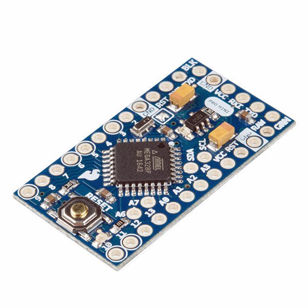
The Arduino Pro Mini is a microcontroller board based on the ATmega328P.
It has 14 digital input/output pins (of which 6 can be used as PWM outputs), 6 analog inputs, an on-board resonator, a reset button, and holes for mounting pin headers. A six pin header can be connected to an FTDI cable or SparkFun breakout board to provide USB power and communication to the board.
The Arduino Pro Mini is intended for semi-permanent installation in objects or exhibitions. The board comes without pre-mounted headers, allowing the use of various types of connectors or direct soldering of wires. The pin layout is compatible with the Arduino Mini.
The Arduino Pro Mini was designed and is manufactured by SparkFun Electronics.
Specifications
Microcontroller
ATmega328P
Board Power Supply
5-12 V
Circuit Operating Voltage
5 V
Digital I/O Pins
14
PWM Pins
6
UART
1
SPI
1
I²C
1
Analog Input Pins
6
External Interrupts
2
DC Current per I/O Pin
40 mA
Flash Memory
32 KB of which 2 KB used by bootloader
SRAM
2 KB
EEPROM
1 KB
Clock Speed
16 MHz
Dimensions
18 x 33.3 mm (0.7 x 1.3")
Downloads
Eagle files
Schematics
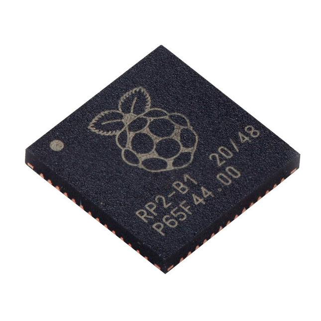
Specifications
Dual ARM Cortex-M0+ @ 133 MHz
264 kB on-chip SRAM in six independent banks
Support for up to 16 MB of off-chip Flash memory via dedicated QSPI bus
DMA controller
Fully-connected AHB crossbar
Interpolator and integer divider peripherals
On-chip programmable LDO to generate core voltage
2x on-chip PLLs to generate USB and core clocks
30x GPIO pins, 4 of which can be used as analogue inputs
Peripherals
2x UARTs
2x SPI controllers
2x I²C controllers
16x PWM channels
USB 1.1 controller and PHY, with host and device support
8x PIO state machines
What you'll get
10x bare RP2040 chips
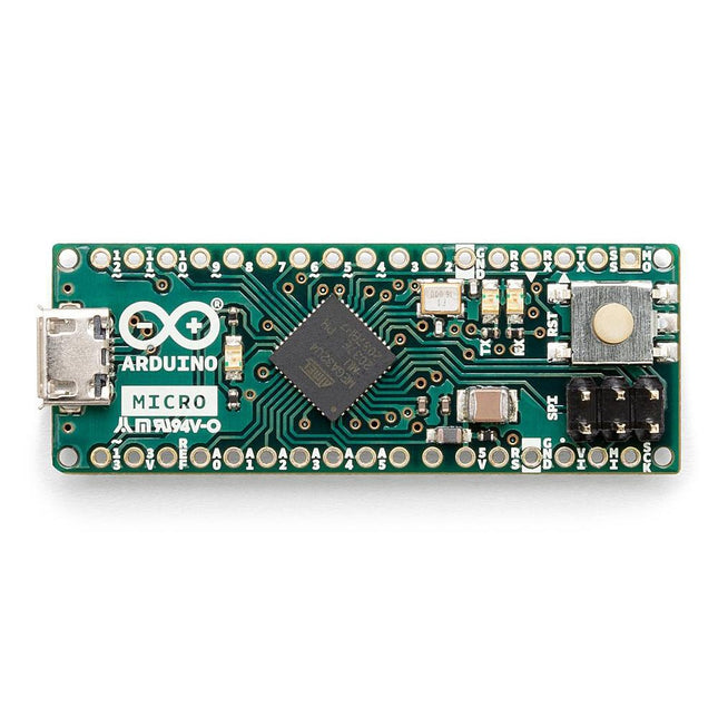
The Arduino Micro contains everything needed to support the microcontroller; simply connect it to a computer with a micro USB cable to get started. It has a form factor that enables it to be easily placed on a breadboard.
The Micro board is similar to the Arduino Leonardo in that the ATmega32U4 has built-in USB communication, eliminating the need for a secondary processor. This allows the Micro to appear to a connected computer as a mouse and keyboard, in addition to a virtual (CDC) serial / COM port.
Specifications
Microcontroller
ATmega32U4
Operating Voltage
5 V
Input Voltage
7 V - 12 V
Analog Input Pins
12
PWM Pins
7
DC I/O Pin
20
DC Current per I/O Pin
20 mA
DC Current for 3.3 V Pin
50 mA
Flash Memory
32 KB of which 4 KB used by the bootloader
SRAM
2.5 KB
EEPROM
1 KB
Clock Speed
16 MHz
LED_Builtin
13
Length
45 mm
Width
18 mm
Weight
13 g
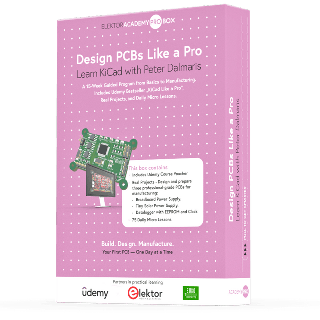
Learn KiCad with Peter Dalmaris
The Academy Pro Box "Design PCBs like a Pro" offers a complete, structured training programme in PCB design, combining online learning with practical application. Based on Peter Dalmaris’ KiCad course, the 15-week programme integrates video lessons, printed materials (2 books), and hands-on projects to ensure participants not only understand the theory but also develop the skills to apply it in practice.
Unlike standard courses, the Academy Pro Box provides a guided learning path with weekly milestones and physical components to design, test, and produce working PCBs. This approach supports a deeper learning experience and better knowledge retention.
The box is ideal for engineers, students, and professionals who want to develop practical PCB design expertise using open-source tools. With the added option to have their final project manufactured, participants complete the programme with real results – ready for use, testing, or further development.
Learn by doing
Build skills. Design real boards. Generate Gerbers. Place your first order. This isn’t just a course – it’s a complete project journey from idea to product.
You’ll walk away with:
Working knowledge of KiCad’s tools
Confidence designing your own PCBs
A fully manufacturable circuit board – made by you
What's inside the Box (Course)?
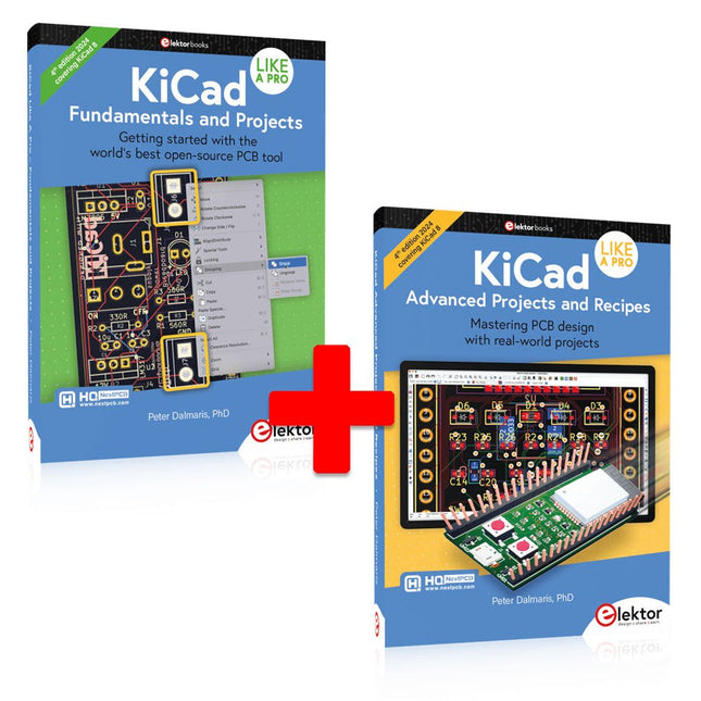
Both volumes of "KiCad Like a Pro" (valued at €105)
Vol 1: Fundamentals and Projects
Vol 2: Advanced Projects and Recipes
Coupon code to join the bestselling KiCad 9 online course by Peter Dalmaris on Udemy, featuring 20+ hours of video training. You'll complete three full design projects:
Breadboard Power Supply
Tiny Solar Power Supply
Datalogger with EEPROM and Clock
Voucher from Eurocircuits for the production of PCBs (worth €85 excl. VAT)
Learning Material (of this Box/Course)
15-Week Learning Program
▶ Click here to open
Week 1: Setup, Fundamentals, and First Steps in PCB Design
Week 2: Starting Your First PCB Project – Schematic Capture
Week 3: PCB Layout – From Netlist to Board Design
Week 4: Design Principles, Libraries, and Workflow
Week 5: Your First Real-World PCB Project
Week 6: Custom Libraries – Symbols, Footprints, and Workflow
Week 7: Advanced Tools – Net Classes, Rules, Zones, Routing
Week 8: Manufacturing Files, BOMs, and PCB Ordering
Week 9: Advanced Finishing Techniques – Graphics, Refinement, and Production Quality
Week 10: Tiny Solar Power Supply – From Schematic to Layout
Week 11: Tiny Solar Power Supply – PCB Layout and Production Prep
Week 12: ESP32 Clone Project – Schematic Design and Layout Prep
Week 13: ESP32 Clone – PCB Layout and Manufacturing Prep
Week 14: Final Improvements and Advanced Features
Week 15: Productivity Tools, Simulation, and Automation
KiCad Course with 18 Lessons on Udemy (by Peter Dalmaris)
▶ Click here to open
Introduction
Getting started with PCB design
Getting started with KiCad
Project: A hands-on tour of KiCad (Schematic Design)
Project: A hands-on tour of KiCad (Layout)
Design principles and PCB terms
Design workflow and considerations
Fundamental KiCad how-to: Symbols and Eeschema
Fundamental KiCad how-to: Footprints and Pcbnew
Project: Design a simple breadboard power supply PCB
Project: Tiny Solar Power Supply
Project: MCU datalogger with build-in 512K EEPROM and clock
Recipes
KiCad 9 new features and improvements
Legacy (from previous versions of KiCad)
KiCad 7 update (Legacy)
(Legacy) Gettings started with KiCad
Bonus lecture
About the Author
Dr. Peter Dalmaris, PhD is an educator, an electrical engineer and Maker. Creator of online video courses on DIY electronics and author of several technical books. As a Chief Tech Explorer since 2013 at Tech Explorations, the company he founded in Sydney, Australia, Peter's mission is to explore technology and help educate the world.
What is Elektor Academy Pro?
Elektor Academy Pro delivers specialized learning solutions designed for professionals, engineering teams, and technical experts in the electronics and embedded systems industry. It enables individuals and organizations to expand their practical knowledge, enhance their skills, and stay ahead of the curve through high-quality resources and hands-on training tools.
From real-world projects and expert-led courses to in-depth technical insights, Elektor empowers engineers to tackle today’s electronics and embedded systems challenges. Our educational offerings include Academy Books, Pro Boxes, Webinars, Conferences, and industry-focused B2B magazines – all created with professional development in mind.
Whether you're an engineer, R&D specialist, or technical decision-maker, Elektor Academy Pro bridges the gap between theory and practice, helping you master emerging technologies and drive innovation within your organization.
The Pro Tech Toolkit is the one thing every DIYer, fixer, hacker, hobbyist, and professional needs to tackle any job.
Every tool in the Pro Tech Toolkit has been re-engineered to be better. From the 64 Bit Driver Kit to the iFixit Opening Picks, every tool is specially designed and selected to maximize your repair capabilities.
At the core of this kit is the iFixit 64 Bit Driver Kit, designed with extensive research into what fastener types are currently used in the consumer electronics industry and which legacy fasteners are still in demand by consumers. From the Apple Watch with its new tiny Tri-Point screws to vintage Nintendo game consoles with gamebit fasteners, the 64 bit kit covers them all with the highest quality CNC machined bits. Even the sturdy case was carefully engineered, having no hinges or latches to break, and features a sorting tray inside the magnetically attached lid.
High-Performance Toolkit for DIY Repairs
The perfect toolkit for pros to average joes.
Contains all the poking, prying, gripping, lifting, ESD safety, and screw driving tools needed to service consumer electronics.
Completely re-engineered to provide all the tools that you need, and none that you don't.
Included
Anti-Static Wrist Strap – protection for circuits against static electricity
Small Suction Handle – suction handle for holding onto things lacking handles
3x iFixit Opening Tool – soft plastic prying tools
6x iFixit Opening Picks – thin prying tool for opening electronic devices
Nylon Tipped Reverse Tweezers – to elevate and hold your work
Angled ESD Tweezers – ESD-safe, feature teeth for tougher grip
Blunt ESD Tweezers – ESD-safe, feature teeth for tougher grip
Standard Spudger – tough antistatic tool for a variety of purposes
Halberd Spudger – features a hook for scooping, scraping, pulling, and guiding.ESD-safe.
Metal Spudger – for more powerful prying, scraping, probing, and poking action
Jimmy – handy tool for 'Jimmy'ing open electronics.
Magnetic Pad – Holds tiny screws and parts during repairs
Tool Roll – Durable and compact
Mako Precision Bit Set – all the bits needed for repairs on small electronics
Mako Precision Bit Set Includes
64 Bit Driver
150 mm Flex Extension
4 mm Screwdriver Bits
Phillips – 000, 00, 0, 1, 2
Flathead – 1, 1.5, 2, 2.5, 3, 4 mm
Torx – T2, T3, T4, T5
Torx Security – TR6, TR7, TR8, TR9, TR10, TR15, TR20, TR25
Pentalobe – P2, P5, P6
JIS – J000, J00, J0, J1
Hex – 0.7, 0.9, 1.3, 1.5, 2, 2.5, 3, 3.5, 4, 4.5, 5 mm
Tri-point – Y000, Y00, Y0, Y1
Nut Driver – 2.5, 3, 3.5, 4, 4.5, 5, 5.5 mm
Square – 1, 2
Gamebit – 3.8, 4.5 mm
Spanner – 6, 8
Triangle – 2, 3 mm
Standoff Bit for iPhone
Oval Bit
Magnetic Pickup Bit
SIM Eject Bit
1/4" to 4 mm Driver Adapter
This bundle includes both volumes of "KiCad Like a Pro" (4th edition 2024). In Fundamentals and Projects (normal price: €49.95), you'll learn how to use KiCad through a practical approach, helping you quickly become productive and start designing your own boards. Advanced Projects and Recipes (normal price: €44.95) allows you to practice your new KiCad skills by challenging yourself with a series of real-world projects.
The latest iteration of KiCad, the world’s best free-to-use Printed Circuit Board tool, is packed with features usually found only in expensive commercial CAD tools. This modern, cross-platform application suite built around schematic and design editors, with auxiliary applications is a stable and mature PCB tool. KiCad 8 is a perfect fit for electronic engineers and makers.
Here are the most significant improvements and features in KiCad 8, both over and under the hood:
Modern user interface, completely redesigned from earlier versions
Improved and customizable electrical and design rule checkers
Theme editor allowing you to customize KiCad on your screen
Ability to import projects from Eagle, CADSTART, and more
Python scripting API
Improved integrated SPICE circuit simulator
Multi-sheet schematics
Filters define selectable elements
Enhanced interactive router helps you draw single tracks and differential pairs with precision
New or enhanced tools to draw tracks, measure distances, tune track lengths, etc.
Advanced interactive router
Built-in bill of materials generator
Realistic ray-tracing capable 3D viewer
Customizable teardrops
Plug-in manager for quick installation of themes, libraries and functionalities such as autorouters and BOM generators
The first book KiCad Like A Pro – Fundamentals and Projects will teach you to use KiCad through a practical approach. It will help you become productive quickly and start designing your own boards. Example projects illustrate the basic features of KiCad, even if you have no prior knowledge of PCB design. The author describes the entire workflow from schematic entry to the intricacies of finalizing the files for PCB production and offers sound guidance on the process.
The second book KiCad Like A Pro – Advanced Projects and Recipes will help you to practice your new KiCad skills by challenging you in a series of real-world projects. The projects are supported by a comprehensive set of recipes with detailed instructions on how to achieve a variety of simple and complex tasks. Design the PCBs for a solar power supply, an LED matrix array, an Arduino-powered datalogger, and a custom ESP32 board. Understand the finer details of the interactive router, how to manage KiCad project teams with Git, how to use an autorouter on 2 and 4-layer PCBs, and much more.
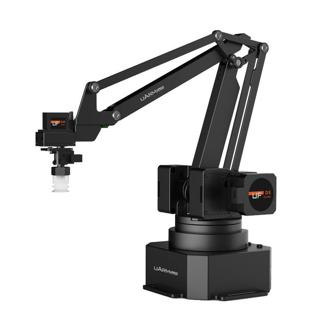
The uArm Swift Pro is a high quality robotic arm that can be used in a wide range of applications. The uArm Swift Pro was developed and optimized for use in education, which means that many packages are already available for open source platforms such as ROS. The uArm Swift Pro has a position repeatability of 0.2 mm and is also equipped with a stepper motor and a 12-bit encoder. These are just a few reasons that make the uArm Swift Pro an excellent choice for educational use. Another great feature is the 3D printing kit that converts the uArm Swift Pro into a 3D printer in less than 1 minute.
The uArm supports the following development platforms/systems:
UFACTORY SDK
Arduino
Python
ROS
GRABCAD
OpenMV
Smartphone App
The smartphone app for iOS is already available in the App Store and enables easy control and monitoring of the robotic arm. The app for Android is in development and will be available soon.
An example of the Machine Vision
The following GIF shows the uArm in combination with the OpenMV Machine Vision Cam M7 and the facial recognition applications that can be implemented in MicroPython.
Specifications
Degrees of Freedom: 4
Repeatability: Up to 0.2 mm
Payload: 500 g
Working Range: 50-320 mm
Positioning Speed: 100 m/s
Position Feedback: 12-bit Encoder
Dimensions: 150 x 140 x 281mm
Weight: 2.2 kg
Included
UFactory uArm Swift Pro Body
Bluetooth & Vacuum Gripper
Downloads
Datasheet
Temporary Delay in the Delivery of Unitree Robots
Like many other suppliers, we are currently experiencing delays in the delivery of Unitree robots. A shipment from our supplier is currently held in customs, which has unfortunately led to later-than-planned deliveries for previously placed orders. We are actively working with our supplier to resolve this issue and expect more clarity soon, but at this time, we cannot provide any guarantees.
Additionally, a new shipment is already on its way, though it will take some time to arrive. Since other suppliers are facing similar challenges, switching to a different provider is unlikely to result in a faster solution. Our top priority remains fulfilling existing orders.
If you have any questions or would like to update your order, please do not hesitate to contact our customer service team. We will keep you informed of any further developments.
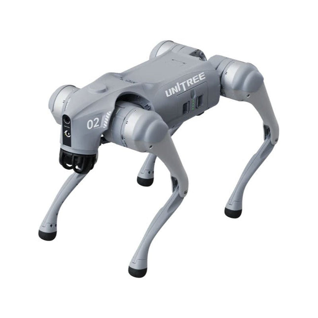
Unitree Go2 series consists of quadruped robots for the research & development of autonomous systems in the fields of human-robot interaction (HRI), SLAM & transportation. Due to the four legs, as well as the 12DOF, this robot can handle a variety of different terrains. The Go2 comes with a perfected drive & power management system, which enables a speed (depending on the version) of up to 3.7 m/s or 11.88 km/h with an operating time of up to 4 hours. Furthermore, the motors have a torque of 45 N.m at the body/thighs and at the knees, which also allow jumps or backflips.
Features
Super Recognition System: 4D LIDAR L1
Max Running Speed: approx. 5 m/s
Peak Joint Torque: approx. 45 N.m
Wireless Module: WiFi 6/Bluetooth/4G
Ultra-long battery Endurance: approx. 2-4 h (long battery life measured in real life)
Intelligent Side-follow System: ISS 2.0
Specifications
Tracking module: Remote-controlled or automatic tracking
Front camera: Image tansmission Resolution 1280x720, FOV 120°, Ultra wide angle lens deliver rich clarity
Front lamp: Brightly lights the way ahead
4D LiDAR L1: 360°x90° omnidirectional ultra-wide-angle scanning allows automatic avoidance with small blind spot and stable operation
12 knee joint motors: Strong and powerful, Beautiful and simple, Brandy new visual experience
Intercom microphone: Effective communication with no scenario restrictions
Self-retracting strap: Easy to carry and load things
More stable, more powerful with advanced devices: 3D LiDAR, 4G ESIM Card, WiFi 6 with Dual-band, Bluetooth 5.2 for stable connection and remote control
Powerful Computing Core: Motion controller, High-performance ARM processor, Improved Al algorithm processor, External ORIN NX/NANO
Smart battery: Standard 8000 mAh battery, Long-endurance 15000 mAh battery, Protection from over-temp, overcharge and short-circuit
Speaker for music play: Listen to music as your pleasure
Unitree Go2 Variants
The Go2 impresses not only with its technical capabilities, but also with a modern and slim design that gives it a futuristic look and makes it a real eye-catcher. The Go2 Air is specially designed for demos and presentations. With its basic features, it offers a solid basis for demonstrating the movement capabilities and functionality of a four-legged robot. Important: The Go2 Air is delivered without a controller. This can be purchased optionally.
With a powerful 8-core high-performance CPU, the Pro and Edu offer impressive computing power required for complex tasks and demanding calculations. This enables faster and more efficient data processing and makes the Pro and Edu a reliable partner for your projects.
From the Edu version onwards, the Go2 is programmable and opens up endless possibilities for developing and researching your own robotics applications. The Go2 is also able to handle a step height of up to 14 cm. This makes it an ideal tool for research, education and entry into the world of robotics.
The Go2 Edu comes with a remote controller that gives you easy and intuitive control. You also get a docking station with impressive computing power of 100 TOPS, which is equipped with powerful AI algorithms and offers you technical support.
Go2 Edu is equipped with a powerful 15000 mAh battery that gives it an impressive runtime of up to 4 hours. This long operating time allows the robot to carry out longer exploration missions and complete demanding tasks.
Model Comparison
Air
Pro
Edu/Edu Plus
Dimensions (standing)
70 x 31 x 40 cm
70 x 31 x 40 cm
70 x 31 x 40 cm
Dimensions (crouching)
76 x 31 x 20 cm
76 x 31 x 20 cm
76 x 31 x 20 cm
Material
Aluminium alloy + High strength engineering plastic
Aluminium alloy + High strength engineering plastic
Aluminium alloy + High strength engineering plastic
Weight (with battery)
about 15 kg
about 15 kg
about 15 kg
Voltage
28~33.6 V
28~33.6 V
28~33.6 V
Peaking capacity
about 3000 W
about 3000 W
about 3000 W
Payload
≈7 kg (MAX ~ 10 kg)
≈8 kg (MAX ~ 10 kg)
≈8 kg (MAX ~ 12 kg)
Speed
0~2.5 m/s
0~3.5 m/s
0~3.7 m/s (MAX ~ 5 m/s)
Max Climb Drop Height
about 15 cm
about 16 cm
about 16 cm
Max Climb Angle
30°
40°
40°
Basic Computing Power
N/A
8-core High-performance CPU
8-core High-performance CPU
Aluminum knee joint motor
12 set
12 set
12 set
Intra-joint circuit (knee)
✓
✓
✓
Joint Heat Pipe Cooler
✓
✓
✓
Range of Motion
Body: −48~48°
Body: −48~48°
Body: −48~48°
Thigh: −200°~90°
Thigh: −200°~90°
Thigh: −200°~90°
Shank: −156°~−48°
Shank: −156°~−48°
Shank: −156°~−48°
Max Torque
N/A
about 45 N.m
about 45 N.m
Super-wide-angle 3D LiDAR
✓
✓
✓
Wireless Vector Positioning Tracking Module
N/A
✓
✓
HD Wide-angle Camera
✓
✓
✓
Foot-end force sensor
N/A
N/A
✓
Basic Action
✓
✓
✓
Auto-scaling strap
N/A
✓
N/A
Upgraded Intelligent OTA
✓
✓
✓
RTT 2.0 Image Transmission
✓
✓
✓
App Basic Remote Control
✓
✓
✓
App Data Viewing
✓
✓
✓
App Graphical Programme
✓
✓
✓
Front Lamp (3 W)
✓
✓
✓
WiFi 6 with Dual-band
✓
✓
✓
Bluetooth 5.2/4.2/2.1
✓
✓
✓
4G Module
N/A
CN/GB
CN/GB
Voice Function
N/A
✓
✓
Music Playback
N/A
✓
✓
ISS 2.0 Intelligent side-follow system
N/A
✓
✓
Intelligent detection and avoidance
✓
✓
✓
Secondary development
N/A
N/A
✓
Manual controller
Optional
Optional
✓
High computing power module
N/A
N/A
Edu: 40 TOPS computing power
Edu Plus: 100 TOPS computing power
NVIDIA Jetson Orin (optional)
Smart Battery
Standard (8000 mAh)
Standard (8000 mAh)
Long endurance (15000 mAh)
Battery Life
1-2 h
1-2 h
2-4 h
Charger
Standard (33.6 V, 3.5 A)
Standard (33.6 V, 3.5 A)
Fast charge (33.6 V, 9 A)
Included
1x Unitree Go2 Pro
1x Unitree Go2 Battery (8000 mAh)
Downloads
Documentation
iOS/Android apps
GitHub
,
by Saad Imtiaz
SparkFun Thing Plus Matter (MGM240P): A Versatile Matter-Based IoT Development Board (Review)
The SparkFun Thing Plus Matter (MGM240P) is a versatile and feature-rich development board designed for creating Matter-based IoT devices. Matter, formerly known as Project CHIP...