The SparkFun RP2040 mikroBUS Development Board is a low-cost, high performance platform with flexible digital interfaces featuring the Raspberry Pi Foundation's RP2040 microcontroller. Besides the Thing Plus or Feather PTH pin layout, the board also includes a microSD card slot, 16 MB (128 Mbit) flash memory, a JST single cell battery connector (with a charging circuit and fuel gauge sensor), an addressable WS2812 RGB LED, JTAG PTH pins, four (4-40 screw) mounting holes, our signature Qwiic connectors, and a mikroBUS socket. The mikroBUS standard was developed by MikroElektronika. Similar to Qwiic and MicroMod interfaces, the mikroBUS socket provides a standardized connection for add-on Click boards to be attached to a development board and is comprised of a pair of 8-pin female headers with a standardized pin configuration. The pins consist of three groups of communications pins (SPI, UART and I²C), six additional pins (PWM, Interrupt, Analog input, Reset and Chip select), and two power groups (3.3 V and 5 V). The RP2040 is supported with both C/C++ and MicroPython cross-platform development environments, including easy access to runtime debugging. It has UF2 boot and floating-point routines baked into the chip. While the chip has a large amount of internal RAM, the board includes an additional 16 MB of external QSPI flash memory to store program code. The RP2040 contains two ARM Cortex-M0+ processors (up to 133 MHz) and features: 264 kB of embedded SRAM in six banks 6 dedicated IO for SPI Flash (supporting XIP) 30 multifunction GPIO: Dedicated hardware for commonly used peripherals Programmable IO for extended peripheral support Four 12-bit ADC channels with internal temperature sensor (up to 0.5 MSa/s) USB 1.1 Host/Device functionality Features (SparkFun RP2040 mikroBUS Dev. Board) Raspberry Pi Foundation's RP2040 microcontroller 18 Multifunctional GPIO Pins Four available 12-bit ADC channels with internal temperature sensor (500kSa/s) Up to eight 2-channel PWM Up to two UARTs Up to two I²C buses Up to two SPI buses Thing Plus (or Feather) Pin Layout: 28 PTH Pins USB-C Connector: USB 1.1 Host/Device functionality 2-pin JST Connector for a LiPo Battery (not included): 500mA charging circuit 4-pin JST Qwiic Connector LEDs:
PWR - Red 3.3V power indicator
CHG - Yellow battery charging indicator
25 - Blue status/test LED (GPIO 25)
WS2812 - Addressable RGB LED (GPIO 08) Buttons: Boot Reset JTAG PTH Pins 16MB QSPI Flash Memory µSD Card Slot mikroBUS Socket Dimensions: 3.7' x 1.2' Four Mounting Holes: 4-40 screw compatible Downloads Schematic Eagle Files Board Dimensions Hookup Guide Qwiic Info Page GitHub Hardware Repository
The CubeCell series is designed primarily for LoRa/LoRaWAN node applications.
Built on the ASR605x platform (ASR6501, ASR6502), these chips integrate the PSoC 4000 series MCU (ARM Cortex-M0+ Core) with the SX1262 module. The CubeCell series offers seamless Arduino compatibility, stable LoRaWAN protocol operation, and straightforward connectivity with lithium batteries and solar panels.
The HTCC-AB02S is a developer-friendly board with an integrated AIR530Z GPS module, ideal for quickly testing and validating communication solutions.
Features
Arduino compatible
Based on ASR605x (ASR6501, ASR6502), those chips are already integrated the PSoC 4000 series MCU (ARM Cortex M0+ Core) and SX1262
LoRaWAN 1.0.2 support
Ultra low power design, 21 uA in deep sleep
Onboard SH1.25-2 battery interface, integrated lithium battery management system (charge and discharge management, overcharge protection, battery power detection, USB/battery power automatic switching)
Good impendence matching and long communication distance
Onboard solar energy management system, can directly connect with a 5.5~7 V solar panel
Micro USB interface with complete ESD protection, short circuit protection, RF shielding, and other protection measures
Integrated CP2102 USB to serial port chip, convenient for program downloading, debugging information printing
Onboard 0.96-inch 128x64 dot matrix OLED display, which can be used to display debugging information, battery power, and other information
Using Air530 GPS module with GPS/Beidou Dual-mode position system support
Specifications
Main Chip
ASR6502 (48 MHz ARM Cortex-M0+ MCU)
LoRa Chipset
SX1262
Frequency
863~870 MHz
Max. TX Power
22 ±1 dBm
Max. Receiving Sensitivity
−135 dBm
Hardware Resource
2x UART1x SPI2x I²C1x SWD3x 12-bit ADC input8-channel DMA engine16x GPIO
Memory
128 Kb FLASH16 Kb SRAM
Power consumption
Deep sleep 21 uA
Interfaces
1x Micro USB1x LoRa Antenna (IPEX)2x (15x 2.54 Pin header) + 3x (2x 2.54 Pin header)
Battery
3.7 V lithium battery (power supply and charging)
Solar Energy
VS pin can be connected to 5.5~7 V solar panel
USB to Serial Chip
CP2102
Display
0.96" OLED (128 x 64)
Operating temperature
−20~70°C
Dimensions
55.9 x 27.9 x 9.5 mm
Included
1x CubeCell HTCC-AB02S Development Board
1x Antenna
1x 2x SH1.25 battery connector
Downloads
Datasheet
Schematic
GPS module (Manual)
Quick start
GitHub
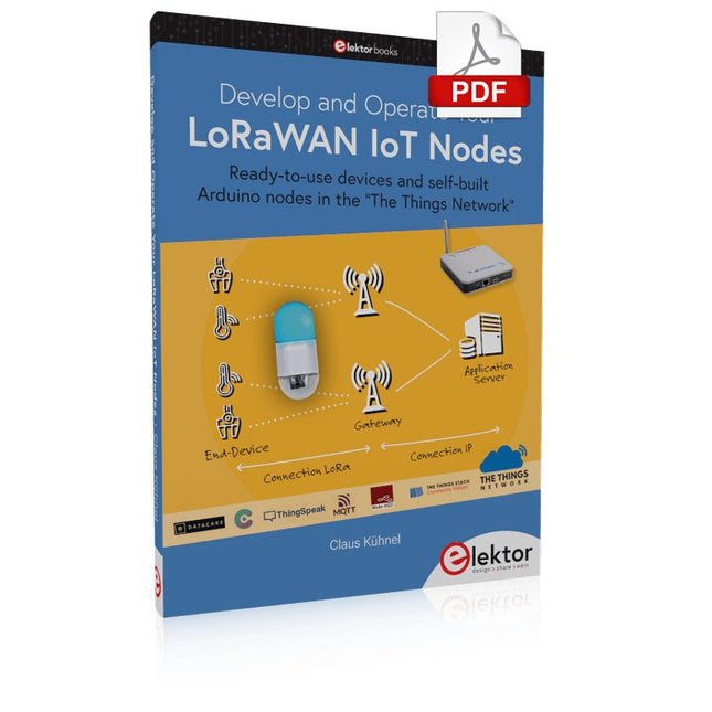
Ready-to-use devices and self-built Arduino nodes in the 'The Things Network'
LoRaWAN has developed excellently as a communication solution in the IoT. The Things Network (TTN) has contributed to this. The Things Network was upgraded to The Things Stack Community Edition (TTS (CE)). The TTN V2 clusters were closed towards the end of 2021.
This book shows you the necessary steps to operate LoRaWAN nodes using TTS (CE) and maybe extend the network of gateways with an own gateway. Meanwhile, there are even LoRaWAN gateways suitable for mobile use with which you can connect to the TTN server via your cell phone.
The author presents several commercial LoRaWAN nodes and new, low-cost and battery-powered hardware for building autonomous LoRaWAN nodes. Registering LoRaWAN nodes and gateways in the TTS (CE), providing the collected data via MQTT and visualization via Node-RED, Cayenne, Thingspeak, and Datacake enable complex IoT projects and completely new applications at very low cost.
This book will enable you to provide and visualize data collected with battery-powered sensors (LoRaWAN nodes) wirelessly on the Internet. You will learn the basics for smart city and IoT applications that enable, for example, the measurement of air quality, water levels, snow depths, the determination of free parking spaces (smart parking), and the intelligent control of street lighting (smart lighting), among others.
The RP2040 utilizes dual ARM Cortex-M0+ processors (up to 133MHz):
264kB of embedded SRAM in six banks
6 dedicated IO for SPI Flash (supporting XIP)
30 multifunction GPIO:
Dedicated hardware for commonly used peripherals
Programmable IO for extended peripheral support
Four 12-bit ADC channels with internal temperature sensor (up to 0.5 MSa/s)
USB 1.1 Host/Device functionality
The RP2040 is supported with C/C++ and MicroPython cross-platform development environments, including easy access to runtime debugging. It has a UF2 boot and floating-point routines baked into the chip. The built-in USB can act as both device and host. It has two symmetric cores and high internal bandwidth, making it useful for signal processing and video. While the chip has a large internal RAM, the board includes an additional external flash chip.
Features
Dual Cortex M0+ processors, up to 133 MHz
264 kB of embedded SRAM in 6 banks
6 dedicated IO for QSPI flash, supporting execute in place (XIP)
30 programmable IO for extended peripheral support
SWD interface
Timer with 4 alarms
Real-time counter (RTC)
USB 1.1 Host/Device functionality
Supported programming languages
MicroPython
C/C++
The Challenger RP2040 NFC is a small embedded computer, equipped with an advanced on-board NFC controller (NXP PN7150), in the popular Adafruit Feather form factor. It is based on an RP2040 microcontroller chip from the Raspberry Pi Foundation which is a dual-core Cortex-M0 that can run on a clock up to 133 MHz.
NFC
The PN7150 is a full featured NFC controller solution with integrated firmware and NCI interface designed for contactless communication at 13.56 MHz. It is fully compatible with NFC forum requirements and is greatly designed based on learnings from previous NXP NFC device generation. It is the ideal solution for rapidly integrating NFC technology in any application, especially small embedded systems reducing Bill of Material (BOM).
The integrated design with full NFC forum compliancy gives the user all the following features:
Embedded NFC firmware providing all NFC protocols as pre-integrated feature.
Direct connection to the main host or microcontroller, by I²C-bus physical and NCI protocol.
Ultra-low power consumption in polling loop mode.
Highly efficient integrated power management unit (PMU) allowing direct supply from a battery.
Specifications
Microcontroller
RP2040 from Raspberry Pi (133 MHz dual-core Cortex-M0)
SPI
One SPI channels configured
I²C
Two I²C channel configured (dedicated I²C for the PN7150)
UART
One UART channel configured
Analog inputs
4 analog input channels
NFC module
PN7150 from NXP
Flash memory
8 MB, 133 MHz
SRAM memory
264 KB (divided into 6 banks)
USB 2.0 controller
Up to 12 MBit/s full speed (integrated USB 1.1 PHY)
JST Battery connector
2.0 mm pitch
On board LiPo charger
450 mA standard charge current
Dimensions
51 x 23 x 3,2 mm
Weight
9 g
Note: Antenna is not included.
Downloads
Datasheet
Quick start example
The LuckFox Pico Ultra is a compact single-board computer (SBC) powered by the Rockchip RV1106G3 chipset, designed for AI processing, multimedia, and low-power embedded applications.
It comes equipped with a built-in 1 TOPS NPU, making it ideal for edge AI workloads. With 256 MB RAM, 8 GB onboard eMMC storage, integrated WiFi, and support for the LuckFox PoE module, the board delivers both performance and versatility across a wide range of use cases.
Running Linux, the LuckFox Pico Ultra supports a variety of interfaces – including MIPI CSI, RGB LCD, GPIO, UART, SPI, I²C, and USB – providing a simple and efficient development platform for applications in smart home, industrial control, and IoT.
Specifications
Chip
Rockchip RV1106G3
Processor
Cortex-A7 1.2 GHz
Neural Network Processor (NPU)
1 TOPS, supports int4, int8, int16
Image Processor (ISP)
Max input 5M @30fps
Memory
256 MB DDR3L
WiFi + Bluetooth
2.4GHz WiFi-6 Bluetooth 5.2/BLE
Camera Interface
MIPI CSI 2-lane
DPI Interface
RGB666
PoE Interface
IEEE 802.3af PoE
Speaker interface
MX1.25 mm
USB
USB 2.0 Host/Device
GPIO
30 GPIO pins
Ethernet
10/100M Ethernet controller and embedded PHY
Default Storage Medium
eMMC (8 GB)
Included
1x LuckFox Pico Ultra W
1x LuckFox PoE module
1x IPX 2.4G 2 db antenna
1x USB-A to USB-C cable
1x Screws pack
Downloads
Wiki
Specifications
Dual ARM Cortex-M0+ @ 133 MHz
264 kB on-chip SRAM in six independent banks
Support for up to 16 MB of off-chip Flash memory via dedicated QSPI bus
DMA controller
Fully-connected AHB crossbar
Interpolator and integer divider peripherals
On-chip programmable LDO to generate core voltage
2x on-chip PLLs to generate USB and core clocks
30x GPIO pins, 4 of which can be used as analogue inputs
Peripherals
2x UARTs
2x SPI controllers
2x I²C controllers
16x PWM channels
USB 1.1 controller and PHY, with host and device support
8x PIO state machines
What you'll get
10x bare RP2040 chips
The ATmega328 Uno Development Board (Arduino Uno compatible) is a microcontroller board based on the ATmega328.
It has 14 digital input/output pins (of which 6 can be used as PWM outputs), 6 analogue inputs, a 16 MHz ceramic resonator, a USB connection, a power jack, an ICSP header and a reset button.
It contains everything needed to support the microcontroller; connect it to a computer with a USB cable or power it with a AC-to-DC adapter or battery to get started.
Specifications
Microcontroller
ATmega328
Operating voltage
5 V DC
Input voltage (recommended)
7-12 V DC
Input voltage (limits)
6-20 V DC
Digital I/O pins
14 (of which 6 provide PWM output)
Analogue input pins
6
SRAM
2 kB (ATmega328)
EEPROM
1 kB (ATmega328)
Flash memory
32 kB (ATmega328) of which 0.5 kB used by bootloader
Clock speed
16 MHz
Downloads
Manual
The FRDM-MCXN947 is a compact and versatile development board designed for rapid prototyping with MCX N94 and N54 microcontrollers. It features industry-standard headers for easy access to the MCU's I/Os, integrated open-standard serial interfaces, external flash memory, and an onboard MCU-Link debugger.
Specifications
Microcontroller
MCX-N947 Dual Arm Cortex-M33 cores @ 150 MHz each with optimized performance efficiency, up to 2 MB dual-bank flash with optional full ECC RAM, External flash
Accelerators: Neural Processing Unit, PowerQuad, Smart DMA, etc.
Memory Expansion
*DNP Micro SD card socket
Connectivity
Ethernet Phy and connector
HS USB-C connectors
SPI/I²C/UART connector (PMOD/mikroBUS, DNP)
WiFi connector (PMOD/mikroBUS, DNP)
CAN-FD transceiver
Debug
On-board MCU-Link debugger with CMSIS-DAP
JTAG/SWD connector
Sensor
P3T1755 I³C/I²C Temp Sensor, Touch Pad
Expansion Options
Arduino Header (with FRDM expansion rows)
FRDM Header
FlexIO/LCD Header
SmartDMA/Camera Header
Pmod *DNP
mikroBUS
User Interface
RGB user LED, plus Reset, ISP, Wakeup buttons
Included
1x FRDM-MCXN947 Development Board
1x USB-C Cable
1x Quick Start Guide
Downloads
Datasheet
Block diagram
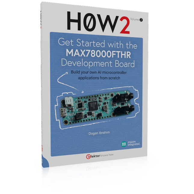
Build your own AI microcontroller applications from scratch
The MAX78000FTHR from Maxim Integrated is a small development board based on the MAX78000 MCU. The main usage of this board is in artificial intelligence applications (AI) which generally require large amounts of processing power and memory. It marries an Arm Cortex-M4 processor with a floating-point unit (FPU), convolutional neural network (CNN) accelerator, and RISC-V core into a single device. It is designed for ultra-low power consumption, making it ideal for many portable AI-based applications.
This book is project-based and aims to teach the basic features of the MAX78000FTHR. It demonstrates how it can be used in various classical and AI-based projects. Each project is described in detail and complete program listings are provided. Readers should be able to use the projects as they are, or modify them to suit their applications. This book covers the following features of the MAX78000FTHR microcontroller development board:
Onboard LEDs and buttons
External LEDs and buttons
Using analog-to-digital converters
I²C projects
SPI projects
UART projects
External interrupts and timer interrupts
Using the onboard microphone
Using the onboard camera
Convolutional Neural Network
This bundle contains:
Book: Get Started with the NXP FRDM-MCXN947 Development Board (normal price: €40)
NXP FRDM-MCXN947 Development Board (normal price: €30)
Book: Get Started with the NXP FRDM-MCXN947 Development Board
Develop projects on connectivity, graphics, machine learning, motor control, and sensors
This book is about the use of the FRDM-MCXN947 Development Board, developed by NXP Semiconductors. It integrates the dual Arm Cortex-M33, operating at up to 150 MHz. Ideal for Industrial, IoT, and machine learning applications. It features Hi-Speed USB, CAN 2.0, I³C and 10/100 Ethernet. The board includes an on-board MCU-Link debugger, FlexI/O for LCD control, and dual-bank flash for read-while-write operations, supporting large external serial memory configurations.
One of the important features of the development board is that it features an integrated eIQ Neutron Neural Processing Unit (NPU), thus enabling users to develop AI-based projects. The development board also supports Arduino Uno form factor header pins, making it compatible with many Arduino shields, mikroBUS connector for MikroElektronika Click Boards, and Pmod connector.
One of the nice things of the FRDM-MCXN947 development board is that it includes several on-board debug probes, allowing programmers to debug their programs by communicating directly with the MCU. With the help of the debugger, programmers can single-step through a program, insert breakpoints, view and modify variables and so on.
Many working and tested projects have been developed in the book using the popular MCUXpresso IDE and the SDK with various sensors and actuators. Use of the popular CMSIS-DSP library is also explained with several commonly used matrix operations.
The projects provided in the book can be used without any modifications in many applications. Alternatively, readers can base their projects on those given in the book during the development of their own projects.
NXP FRDM-MCXN947 Development Board
The FRDM-MCXN947 is a compact and versatile development board designed for rapid prototyping with MCX N94 and N54 microcontrollers. It features industry-standard headers for easy access to the MCU's I/Os, integrated open-standard serial interfaces, external flash memory, and an onboard MCU-Link debugger.
Specifications
Microcontroller
MCX-N947 Dual Arm Cortex-M33 cores @ 150 MHz each with optimized performance efficiency, up to 2 MB dual-bank flash with optional full ECC RAM, External flash
Accelerators: Neural Processing Unit, PowerQuad, Smart DMA, etc.
Memory Expansion
*DNP Micro SD card socket
Connectivity
Ethernet Phy and connector
HS USB-C connectors
SPI/I²C/UART connector (PMOD/mikroBUS, DNP)
WiFi connector (PMOD/mikroBUS, DNP)
CAN-FD transceiver
Debug
On-board MCU-Link debugger with CMSIS-DAP
JTAG/SWD connector
Sensor
P3T1755 I³C/I²C Temp Sensor, Touch Pad
Expansion Options
Arduino Header (with FRDM expansion rows)
FRDM Header
FlexIO/LCD Header
SmartDMA/Camera Header
Pmod *DNP
mikroBUS
User Interface
RGB user LED, plus Reset, ISP, Wakeup buttons
Included
1x FRDM-MCXN947 Development Board
1x USB-C Cable
1x Quick Start Guide
Downloads
Datasheet
Block diagram
The Challenger RP2040 WiFi is a small embedded computer equipped with a WiFi module, in the popular Adafruit Feather form factor. It is based on an RP2040 microcontroller chip from the Raspberry Pi Foundation which is a dual-core Cortex-M0 that can run on a clock up to 133 MHz.
The RP2040 is paired with a 8 MB high-speed flash capable of supplying data up to the max speed. The flash memory can be used both to store instructions for the microcontroller as well as data in a file system and having a file system available makes it easy to store data in a structured and easy to program approach.
The device can be powered from a Lithium Polymer battery connected through a standard 2.0 mm connector on the side of the board. An internal battery charging circuit allows you to charge your battery safely and quickly. The device is shipped with a programming resistor that sets the charging current to 250 mA. This resistor can be exchanged by the user to either increase or decrease the charging current, depending on the battery that is being used.
The WiFi section on this board is based on the Espressif ESP8285 chip which basically is a ESP8266 with 1 MB flash memory integrated onto the chip making it a complete WiFi only requiring very few external components.
The ESP8285 is connected to the microcontroller using a UART channel and the operation is controlled using a set of standardized AT-commands.
Specifications
Microcontroller
RP2040 from Raspberry Pi (133 MHz dual-core Cortex-M0)
SPI
One SPI channel configured
I²C
One I²C channel configured
UART
One UART channel configured (second UART is for the WiFi chip)
Analog inputs
4 analog input channels
WLAN controller
ESP8285 from Espressif (160 MHz single-core Tensilica L106)
Flash memory
8 MByte, 133 MHz
SRAM memory
264 KByte (divided into 6 banks)
USB 2.0 controller
Up to 12 MBit/s full speed (integrated USB 1.1 PHY)
JST Battery connector
2.0 mm pitch
Onboard LiPo charger
250 mA standard charge current
Onboard NeoPixel LED
RGB LED
Dimensions
51 x 23 x 3,2 mm
Weight
9 g
Downloads
Datasheet
Design files
Product errata