With the availability of free and open source C/C++ compilers today, you might wonder why someone would be interested in assembler language. What is so compelling about the RISC-V Instruction Set Architecture (ISA)? How does RISC-V differ from existing architectures? And most importantly, how do we gain experience with the RISC-V without a major investment? Is there affordable hardware available?
The availability of the Espressif ESP32-C3 chip provides a way to get hands-on experience with RISC-V. The open sourced QEMU emulator adds a 64-bit experience in RISC-V under Linux. These are just two ways for the student and enthusiast alike to explore RISC-V in this book.
The projects in this book are boiled down to the barest essentials to keep the assembly language concepts clear and simple. In this manner you will have “aha!” moments rather than puzzling about something difficult. The focus in this book is about learning how to write RISC-V assembly language code without getting bogged down. As you work your way through this tutorial, you’ll build up small demonstration programs to be run and tested. Often the result is some simple printed messages to prove a concept. Once you’ve mastered these basic concepts, you will be well equipped to apply assembly language in larger projects.
The FRDM-MCXN947 is a compact and versatile development board designed for rapid prototyping with MCX N94 and N54 microcontrollers. It features industry-standard headers for easy access to the MCU's I/Os, integrated open-standard serial interfaces, external flash memory, and an onboard MCU-Link debugger.
Specifications
Microcontroller
MCX-N947 Dual Arm Cortex-M33 cores @ 150 MHz each with optimized performance efficiency, up to 2 MB dual-bank flash with optional full ECC RAM, External flash
Accelerators: Neural Processing Unit, PowerQuad, Smart DMA, etc.
Memory Expansion
*DNP Micro SD card socket
Connectivity
Ethernet Phy and connector
HS USB-C connectors
SPI/I²C/UART connector (PMOD/mikroBUS, DNP)
WiFi connector (PMOD/mikroBUS, DNP)
CAN-FD transceiver
Debug
On-board MCU-Link debugger with CMSIS-DAP
JTAG/SWD connector
Sensor
P3T1755 I³C/I²C Temp Sensor, Touch Pad
Expansion Options
Arduino Header (with FRDM expansion rows)
FRDM Header
FlexIO/LCD Header
SmartDMA/Camera Header
Pmod *DNP
mikroBUS
User Interface
RGB user LED, plus Reset, ISP, Wakeup buttons
Included
1x FRDM-MCXN947 Development Board
1x USB-C Cable
1x Quick Start Guide
Downloads
Datasheet
Block diagram
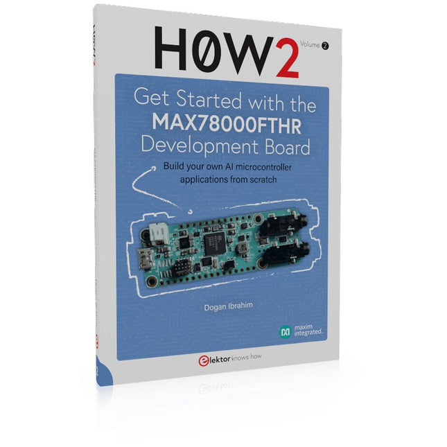
Build your own AI microcontroller applications from scratch
The MAX78000FTHR from Maxim Integrated is a small development board based on the MAX78000 MCU. The main usage of this board is in artificial intelligence applications (AI) which generally require large amounts of processing power and memory. It marries an Arm Cortex-M4 processor with a floating-point unit (FPU), convolutional neural network (CNN) accelerator, and RISC-V core into a single device. It is designed for ultra-low power consumption, making it ideal for many portable AI-based applications.
This book is project-based and aims to teach the basic features of the MAX78000FTHR. It demonstrates how it can be used in various classical and AI-based projects. Each project is described in detail and complete program listings are provided. Readers should be able to use the projects as they are, or modify them to suit their applications. This book covers the following features of the MAX78000FTHR microcontroller development board:
Onboard LEDs and buttons
External LEDs and buttons
Using analog-to-digital converters
I²C projects
SPI projects
UART projects
External interrupts and timer interrupts
Using the onboard microphone
Using the onboard camera
Convolutional Neural Network
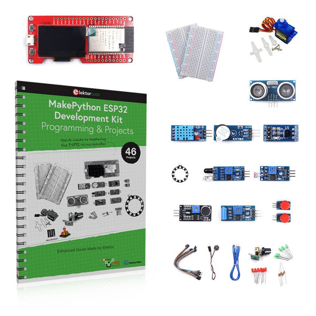
Learn how to use the ESP32 Microcontroller and MicroPython programming in your future projects!
The project book, written by well-known Elektor author Dogan Ibrahim, holds many software- and hardware-based projects especially developed for the MakePython ESP32 Development Kit. The kit comes with several LEDs, sensors, and actuators. The kit will help you acquire the basic knowledge to create IoT projects.
The book’s fully evaluated projects feature all the supplied components. Each project includes a block diagram, a circuit diagram, a full program listing, and a complete program description.
Included in the kit
1x MakePython ESP32 development board with LCD
1x Ultrasonic ranging module
1x Temperature and humidity sensor
1x Buzzer module
1x DS18B20 module
1x Infrared module
1x Potentiometer
1x WS2812 module
1x Sound sensor
1x Vibration sensor
1x Photosensitive resistance module
1x Pulse sensor
1x Servo motor
1x USB cable
2x Button
2x Breadboard
45x Jumper wire
10x Resistor 330R
10x LED (Red)
10x LED (Green)
1x Project book (206 pages)
46 Projects in the Book
LED Projects
Blinking LED
Flashing SOS
Blinking LED – using a timer
Alternately flashing LEDs
Button control
Changing the LED flashing rate using pushbutton interrupts
Chasing-LEDs
Binary-counting LEDs
Christmas lights (random-flashing 8 LEDs)
Electronic dice
Lucky day of the week
Pulsewidth Modulation (PWM) Projects
Generate a 1000-Hz PWM waveform with 50% duty cycle
LED brightness control
Measuring the frequency and duty cycle of a PWM waveform
Melody maker
Simple electronic organ
Servo motor control
Servo motor DS18B20 thermometer
Analog To Digital Converter (ADC) Projects
Voltmeter
Plotting the analog input voltage
ESP32 internal temperature sensor
Ohmmeter
Photosensitive resistance module
Digital To Analog Converter (DAC) Projects
Generating fixed voltages
Generating a sawtooth-wave signal
Generating a triangular-wave signal
Arbitrary periodic waveform
Generating a sinewave signal
Generating accurate sinewave signal using timer interrupts
Using The OLED Display
Seconds counter
Event counter
DS18B20 OLED based digital thermometer
ON-OFF temperature controller
Measuring the temperature and humidity
Ultrasonic distance measurement
Height of a person (stadiometer)
Heart rate (pulse) measurement
Other Sensors Supplied with the Kit
Theft alarm
Sound-activated light
Infrared obstacle avoidance with buzzer
WS2812 RGB LED ring
Timestamping temperature and humidity readings
Network Programming
Wi-Fi scanner
Remote control from the Internet browser (using a smartphone or PC) – Web Server
Storing temperature and humidity data in the Cloud
Low-Power Operation
Using a timer to wake up the processor
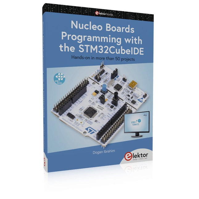
Hands-on in more than 50 projects
STM32 Nucleo family of processors are manufactured by STMicroelectronics. These are low-cost ARM microcontroller development boards. This book is about developing projects using the popular STM32CubeIDE software with the Nucleo-L476RG development board. In the early Chapters of the book the architecture of the Nucleo family is briefly described.
The book covers many projects using most features of the Nucleo-L476RG development board where the full software listings for the STM32CubeIDE are given for each project together with extensive descriptions. The projects range from simple flashing LEDs to more complex projects using modules, devices, and libraries such as GPIO, ADC, DAC, I²C, SPI, LCD, DMA, analogue inputs, power management, X-CUBE-MEMS1 library, DEBUGGING, and others. In addition, several projects are given using the popular Nucleo Expansion Boards. These Expansion Boards plug on top of the Nucleo development boards and provide sensors, relays, accelerometers, gyroscopes, Wi-Fi, and many others. Using an expansion board together with the X-CUBE-MEMS1 library simplifies the task of project development considerably.
All the projects in the book have been tested and are working. The following sub-headings are given for each project: Project Title, Description, Aim, Block Diagram, Circuit Diagram, and Program Listing for the STM32CubeIDE.
In this book you will learn about
STM32 microcontroller architecture;
the Nucleo-L476RG development board in projects using the STM32CubeIDE integrated software development tool;
external and internal interrupts and DMA;
DEBUG, a program developed using the STM32CubeIDE;
the MCU in Sleep, Stop, and in Standby modes;
Nucleo Expansion Boards with the Nucleo development boards.
What you need
a PC with Internet connection and a USB port;
STM32CubeIDE software (available at STMicroelectronics website free of charge)
the project source files, available from the book’s webpage hosted by Elektor;
Nucleo-L476RG development board;
simple electronic devices such as LEDs, temperature sensor, I²C and SPI chips, and a few more;
Nucleo Expansion Boards (optional).
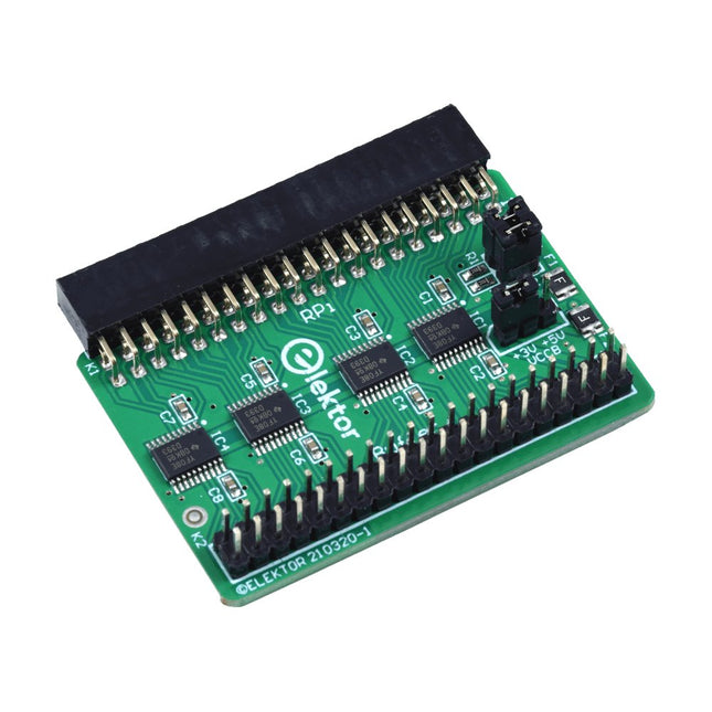
When you experiment with the Raspberry Pi on a regular basis and you connect a variety of external hardware to the GPIO port via the header you may well have caused some damage in the past. The Elektor Raspberry Pi Buffer Board is there to prevent this! The board is compatible with Raspberry Pi Zero, Zero 2 (W), 3, 4, 5, 400 and 500.
All 26 GPIOs are buffered with bi-directional voltage translators to protect the Raspberry Pi when experimenting with new circuits. The PCB is intended to be inserted in the back of Raspberry Pi 400/500. The connector to connect to the Raspberry Pi is a right angled 40-way receptacle (2x20). The PCB is only a fraction wider. A 40-way flat cable with appropriate 2x20 headers can be connected to the buffer output header to experiment for instance with a circuit on a breadboard or PCB.
The circuit uses 4x TXS0108E ICs by Texas Instruments. The PCB can also be put upright on a Raspberry Pi.
Downloads
Schematics
Layout
STM32 Nucleo family of processors are manufactured by STMicroelectronics. These are low-cost ARM microcontroller development boards. This book is about developing projects using the popular Nucleo development board. In the early chapters of the book, the architecture of the Nucleo family is briefly described.
Software development tools that can be used with the Nucleo boards such as the Mbed, Keil MDK, TrueSTUDIO, and the System Workbench are described briefly in later Chapters.
The book covers many projects using most features of the STM32 Nucleo development boards where the full software listings for Mbed and System Workbench are given for every project. The projects range from simple flashing LEDs to more complex projects using modules and devices such as GPIO, ADC, DAC, I²C, LCD, analog inputs and others.
In addition, several projects are given using the Nucleo Expansion Boards, including popular expansion boards such as solid-state relay, MEMS and environmental sensors, DC motor driver, Wi-Fi, and stepper motor driver.
These Expansion Boards plug on top of the Nucleo development boards and simplify the task of project development considerably.
Features of this book
Learn the architecture of the STM32 microcontrollers
Learn how to use the Nucleo development board in projects using Mbed and System Workbench Toolchains
Learn how to use the Nucleo Expansion Boards with the Nucleo development boards
Update
The Mbed compiler has been replaced with two software packages: The Mbed Studio and Keil Studio Cloud. Both of these software packages are free of charge and are available on the Internet. If you need assistance using the Keil Studio Cloud, please download the Guide below.
Features
Build in USB to Serial interface
Build-in PCB antenna
Powered by Pineseed BL602 SoC using Pinenut model: 12S stamp
2 MB Flash
USB-C connection
Suitable to breadboard BIY project
On board three color LEDs output
Dimensions: 25.4 x 44.0 mm
Note: USB cable is not included.
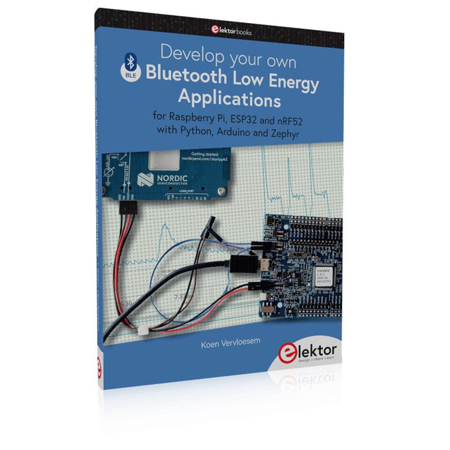
For Raspberry Pi, ESP32 and nRF52 with Python, Arduino and Zephyr
Bluetooth Low Energy (BLE) radio chips are ubiquitous from Raspberry Pi to light bulbs. BLE is an elaborate technology with a comprehensive specification, but the basics are quite accessible.
A progressive and systematic approach will lead you far in mastering this wireless communication technique, which is essential for working in low power scenarios.
In this book, you’ll learn how to:
Discover BLE devices in the neighborhood by listening to their advertisements.
Create your own BLE devices advertising data.
Connect to BLE devices such as heart rate monitors and proximity reporters.
Create secure connections to BLE devices with encryption and authentication.
Understand BLE service and profile specifications and implement them.
Reverse engineer a BLE device with a proprietary implementation and control it with your own software.
Make your BLE devices use as little power as possible.
This book shows you the ropes of BLE programming with Python and the Bleak library on a Raspberry Pi or PC, with C++ and NimBLE-Arduino on Espressif’s ESP32 development boards, and with C on one of the development boards supported by the Zephyr real-time operating system, such as Nordic Semiconductor's nRF52 boards.
Starting with a very little amount of theory, you’ll develop code right from the beginning. After you’ve completed this book, you’ll know enough to create your own BLE applications.
Hands-on in more than 50 projects
STM32 Nucleo family of processors are manufactured by STMicroelectronics. These are low-cost ARM microcontroller development boards. This book is about developing projects using the popular STM32CubeIDE software with the Nucleo-L476RG development board. In the early Chapters of the book the architecture of the Nucleo family is briefly described.
The book covers many projects using most features of the Nucleo-L476RG development board where the full software listings for the STM32CubeIDE are given for each project together with extensive descriptions. The projects range from simple flashing LEDs to more complex projects using modules, devices, and libraries such as GPIO, ADC, DAC, I²C, SPI, LCD, DMA, analogue inputs, power management, X-CUBE-MEMS1 library, DEBUGGING, and others. In addition, several projects are given using the popular Nucleo Expansion Boards. These Expansion Boards plug on top of the Nucleo development boards and provide sensors, relays, accelerometers, gyroscopes, Wi-Fi, and many others. Using an expansion board together with the X-CUBE-MEMS1 library simplifies the task of project development considerably.
All the projects in the book have been tested and are working. The following sub-headings are given for each project: Project Title, Description, Aim, Block Diagram, Circuit Diagram, and Program Listing for the STM32CubeIDE.
In this book you will learn about
STM32 microcontroller architecture;
the Nucleo-L476RG development board in projects using the STM32CubeIDE integrated software development tool;
external and internal interrupts and DMA;
DEBUG, a program developed using the STM32CubeIDE;
the MCU in Sleep, Stop, and in Standby modes;
Nucleo Expansion Boards with the Nucleo development boards.
What you need
a PC with Internet connection and a USB port;
STM32CubeIDE software (available at STMicroelectronics website free of charge)
the project source files, available from the book’s webpage hosted by Elektor;
Nucleo-L476RG development board;
simple electronic devices such as LEDs, temperature sensor, I²C and SPI chips, and a few more;
Nucleo Expansion Boards (optional).